Datasheet Summary
HEF4094B
8-stage shift-and-store register
Rev. 15
- 5 September 2024
Product data sheet
1. General description
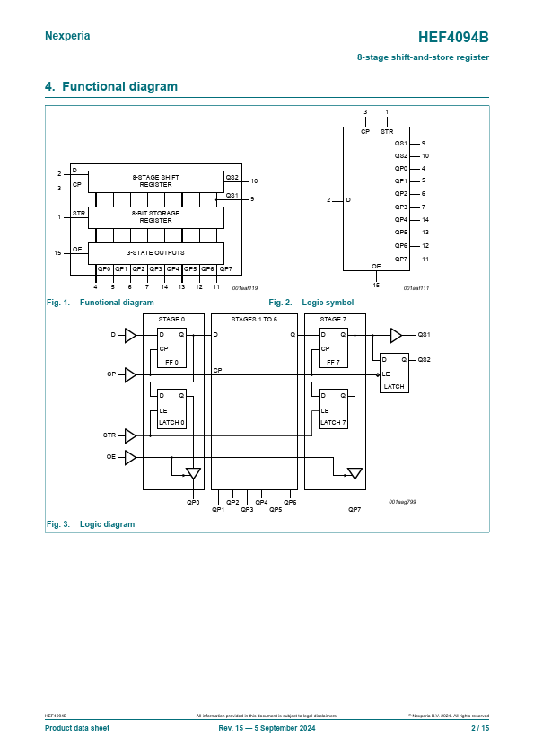
The HEF4094B is an 8-bit serial-in/serial or parallel-out shift register with a storage register and 3-state outputs. Both the shift and storage register have separate clocks. The device Features a serial input (D) and two serial outputs (QS1 and QS2) to enable cascading. Data is shifted on the LOW-to-HIGH transitions of the CP input. Data is available at QS1 on the LOW-to-HIGH transitions of the CP input to allow cascading when clock edges are fast. The same data is available at QS2 on the next HIGH-to-LOW transition of the CP input to allow cascading when clock edges are slow....