Datasheet4U Logo Datasheet4U.com

NXB0104PW-Q100 - Dual supply translating transceiver

Download the NXB0104PW-Q100 datasheet PDF. This datasheet also covers the NXB0104-Q100 variant, as both devices belong to the same dual supply translating transceiver family and are provided as variant models within a single manufacturer datasheet.

General Description

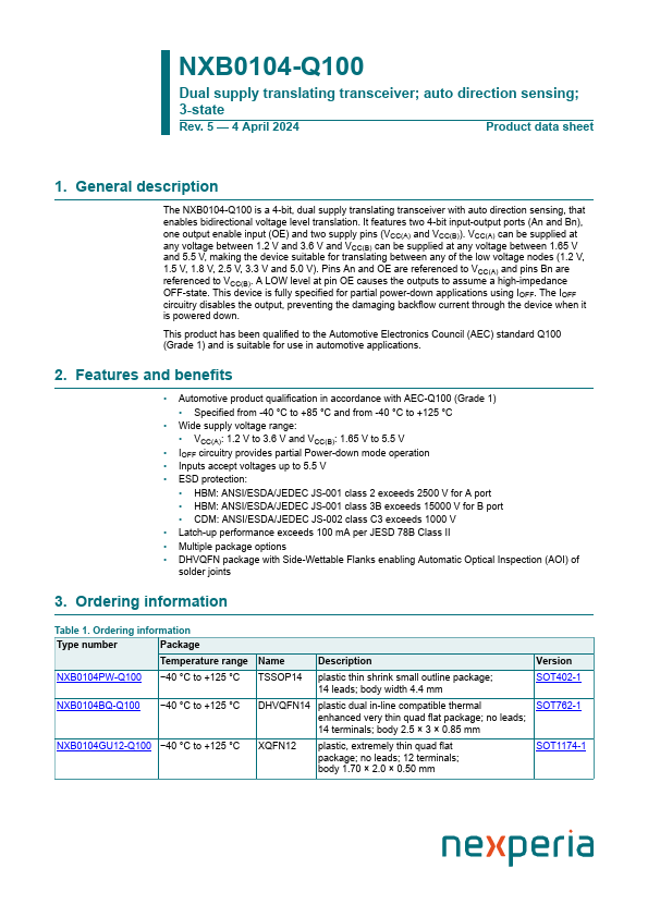
The NXB0104-Q100 is a 4-bit, dual supply translating transceiver with auto direction sensing, that enables bidirectional voltage level translation.

Key Features

  • Automotive product qualification in accordance with AEC-Q100 (Grade 1).
  • Specified from -40 °C to +85 °C and from -40 °C to +125 °C.
  • Wide supply voltage range:.
  • VCC(A): 1.2 V to 3.6 V and VCC(B): 1.65 V to 5.5 V.
  • IOFF circuitry provides partial Power-down mode operation.
  • Inputs accept voltages up to 5.5 V.
  • ESD protection:.
  • HBM: ANSI/ESDA/JEDEC JS-001 class 2 exceeds 2500 V for A port.
  • HBM: ANSI/ESDA/JEDEC JS-001 cla.

📥 Download Datasheet

Note: The manufacturer provides a single datasheet file (NXB0104-Q100-nexperia.pdf) that lists specifications for multiple related part numbers.

Full PDF Text Transcription for NXB0104PW-Q100 (Reference)

Note: Below is a high-fidelity text extraction (approx. 800 characters) for NXB0104PW-Q100. For precise diagrams, and layout, please refer to the original PDF.

NXB0104-Q100 Dual supply translating transceiver; auto direction sensing; 3-state Rev. 5 — 4 April 2024 Product data sheet 1. General description The NXB0104-Q100 is a 4-...

View more extracted text
024 Product data sheet 1. General description The NXB0104-Q100 is a 4-bit, dual supply translating transceiver with auto direction sensing, that enables bidirectional voltage level translation. It features two 4-bit input-output ports (An and Bn), one output enable input (OE) and two supply pins (VCC(A) and VCC(B)). VCC(A) can be supplied at any voltage between 1.2 V and 3.6 V and VCC(B) can be supplied at any voltage between 1.65 V and 5.5 V, making the device suitable for translating between any of the low voltage nodes (1.2 V, 1.5 V, 1.8 V, 2.5 V, 3.3 V and 5.0 V). Pins An and OE are referenced to VCC(A) and pins Bn are