DESCRIPTION
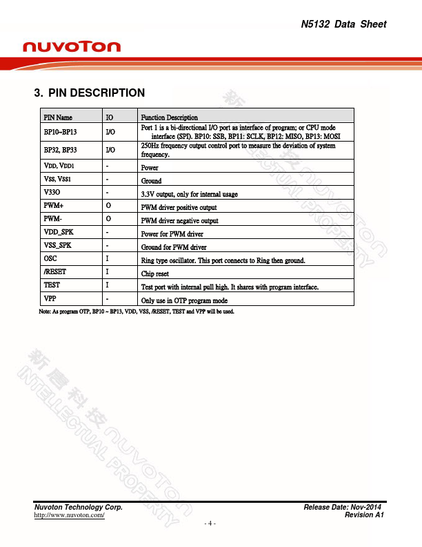
PIN Name BP10~BP13 BP32, BP33 IO Function DESCRIPTION
I/O Port 1 is a bi-directional I/O port as interface of program; or CPU mode interface (SPI). BP10: SSB, BP11: SCLK, BP12: MISO, BP13: MOSI I/O 250Hz frequency output control port to measure the deviation of system frequency. VDD, VDD1 - Power VSS, VSS1 - Ground V33O - 3.3V output, only for internal usage PWM+ O PWM driver positive output PWM- O PWM driver negative output VDD_SPK - Power for PWM driver VSS_SPK - Ground for PWM driver OSC I Ring type oscillator. This port connects to Ring then ground. /RESET I Chip reset TEST I Test port with internal pull high. It shares with program interface. VPP - Only use in OTP program mode Note: As program OTP, BP10 ~ BP13, VDD, VSS, /RESET, TEST and VPP will be used. Nuvoton Technology Corp. -4- Release Date: Nov-2014 Revision A1 N5132 Data Sheet 4. DC/AC CHARACTERISTICS 4.1 Absolute maximum ratings PARAMETER Power Supply Input Voltage Storage Temperature Operating Temperature SYM... Nuvoton Technology