onsemi 10EL34
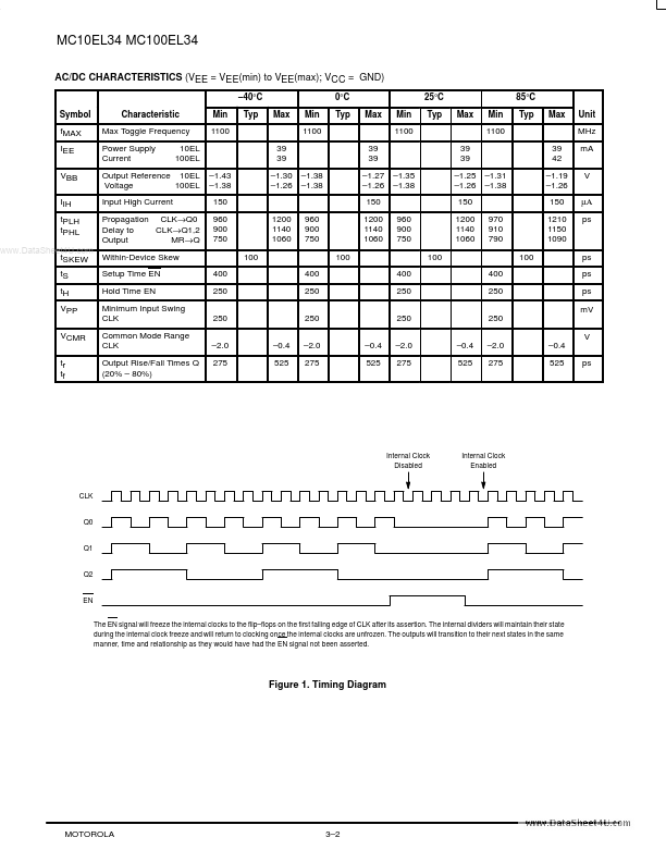
The EN signal will freeze the internal clocks to the flip–flops on the first falling edge of CLK after its assertion. The internal dividers will maintain their state during the internal clock freeze and will return to clocking once the internal clocks are unfrozen.| Part No. | 10EL34 |
|---|---|
| Datasheet | 10EL34 Download |
| Manufacturer |  onsemi |
| Description | MC10EL34 |
| Buy | Stock & Price |
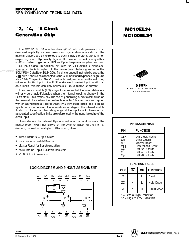
DESCRIPTION
PIN CLK EN MR VBB Q0 Q1 Q2 FUNCTION Diff Clock Inputs Sync Enable Master Reset Reference Output Diff ÷2 Outputs Diff ÷4 Outputs Diff ÷8 Outputs FUNCTION TABLE●
●
●
●
● 50ps Output-to-Output Skew Synchronous Enable/Disable Master Reset for Synchronization 75kΩ Internal Input Pulldown Resistors >1000V ESD Protection LOGIC DIAGRAM AND PINOUT ASSIGNMENT CLK VCC 16 EN 15 D Q ÷2 Q R NC 14 CLK 13 CLK 12 VBB 11 MR 10 VEE 9 EN L H X MR L L H FUNCTION Divide Hold Q0–3 Reset Q0–3 Z ZZ X R ÷4 Q R ÷8 Q R Z = Low-to-High Transition ZZ = High-to-Low Transition 1 Q0 2 Q0 3 VCC 4 Q1 5 Q1 6 VCC 7 Q2 8 Q2 12/93 © Motorola, Inc. 1996 3–1 REV 2 MC10EL34 MC100EL34 AC/DC CHARACTERISTICS (VEE = VEE(min) to VEE(max); VCC = GND) –40°C Symbol fMAX IEE VBB IIH tPLH tPHL Characteristic Max Toggle Frequency Power Supply Current 10EL 100EL –1.43 –1.38 150 960 900 750 100 400 250 250 –2.0 275 –0.4 525 400 250 250 –2.0 275 –0.4 525 1200 1140 1060 960 900 750 100 400 250 250 –2.0 275 –0.4 525 Min 1100 39 3...