onsemi 2N4923
1 AMPERE GENERAL PURPOSE POWER TRANSISTORS
| Part No. | 2N4923 |
|---|---|
| Datasheet | 2N4923 Download |
| Manufacturer |  onsemi |
| Description | 1 AMPERE GENERAL PURPOSE POWER TRANSISTORS |
| Buy | Stock & Price |
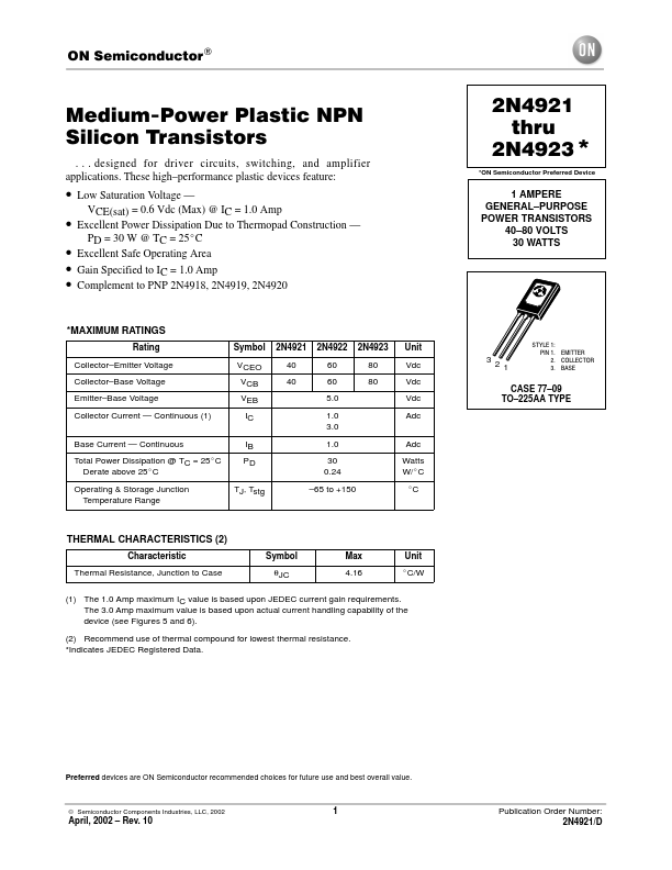
MAXIMUM RATINGS
Rating Symbol VCEO VCB VEB IC IB 2N4921 40 40 2N4922 60 60 2N4923 80 80 Unit Vdc Vdc Vdc Adc Adc Collector–Emitter Voltage Collector–Base Voltage Emitter–Base Voltage 5.0 1.0 3.0 1.0 Collector Current — Continuous (1) Base Current — Continuous Total Power Dissipation @ TC = 25_C Derate above 25_C Operating & Storage Junction Temperature Range PD 30 0.24 Watts W/_C _C TJ, Tstg –65 to +150 3 2 1 STYLE 1: PIN 1. EMITTER 2. COLLECTOR 3. BASE CASE 77–09 TO–225AA TYPE THERMAL CHARACTERISTICS (2) Characteristic Symbol θJC Max Unit Thermal Resistance, Junction to Case 4.16 _C/W (1) The 1.0 Amp maximum IC value is based upon JEDEC current gain requirements. The 3.0 Amp maximum value is based upon actual current handling capability of the device (see Figures 5 and 6). (2) Recommend use of thermal compound for lowest thermal resistance. *Indicates JEDEC Registered Data. Preferred devices are ON Semiconductor recommended choices for future use and best overall value. © Semiconductor Components Industries, LLC, 2002 1 April, 2002 – Rev.