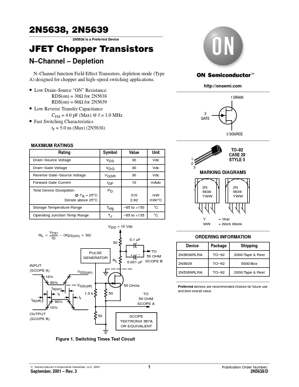
MAXIMUM RATINGS
Rating Drain–Source Voltage Drain–Gate Voltage Reverse Gate–Source Voltage Forward Gate Current Total Device Dissipation @ TA = 25°C Derate above 25°C Storage Temperature Range Operating Junction Temp Range Symbol VDS VDG VGSR IGF PD 310 2.82 Tstg TJ –65 to +150 –65 to +135 mW mW/°C °C °C Y WW = Year = Work Week Value 30 30 30 10 Unit Vdc Vdc Vdc mAdc 2N 5638 YWW 2N 5639 YWW 1 2 3 TO–92 CASE 29 STYLE 5 MARKING DIAGRAMS VDD = 10 Vdc V RL + DD * (RDS(on) ) 50) ID 50 PULSE GENERATOR INPUT (SCOPE A) 10% 90% td(on) tf td(off) OUTPUT (SCOPE B) 90% 10% 50 SCOPE TEKTRONIX 567A OR EQUIVALENT 0.1 mF TO + – 50 OHM 0.001 mF SCOPE B ORDERING INFORMATION Device 2N5638RLRA 2N5639 2N5369RLRA Package TO–92 TO–92 TO–92 Shipping 2000/Tape & Reel 5000/Box 2000/Tape & Reel RL VGS(on) VGS(off) 1.0 k tr 50 50 Ohms TO 50 OHM SCOPE A Preferred devices are recommended choices for future use and best overall value. Figure 1. Switching Times Test Circuit © Semiconductor Components Industries, LLC, 2001 1 September, 2001 – Rev. onsemi