onsemi 2N5555
Switching JFET
| Part No. | 2N5555 |
|---|---|
| Datasheet | 2N5555 Download |
| Manufacturer |  onsemi |
| Description | Switching JFET |
| Buy | Stock & Price |
MAXIMUM RATINGS
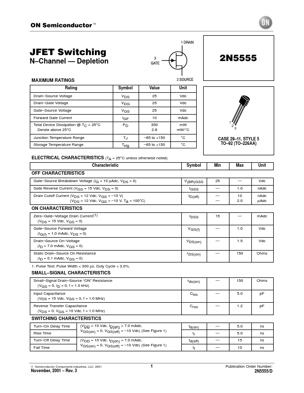
Rating Drain–Source Voltage Drain–Gate Voltage Gate–Source Voltage Forward Gate Current Total Device Dissipation @ TC = 25°C Derate above 25°C Junction Temperature Range Storage Temperature Range Symbol VDS VDG VGS IGF PD TJ Tstg Value 25 25 25 10 350 2.8 –65 to +150 –65 to +150 2 SOURCE Unit Vdc Vdc Vdc mAdc mW mW/°C °C °CELECTRICAL CHARACTERISTICS
(TA = 25°C unless otherwise noted) Characteristic OFF CHARACTERISTICS Gate–Source Breakdown Voltage (IG = 10 µAdc, VDS = 0) Gate Reverse Current (VGS = 15 Vdc, VDS = 0) Drain Cutoff Current (VDS = 12 Vdc, VGS = –10 V) Drain Cutoff Current (VDS = 12 Vdc, VGS = –10 V, TA = 100°C) ON CHARACTERISTICS Zero–Gate–Voltage Drain Current(1) (VDS = 15 Vdc, VGS = 0) Gate–Source Forward Voltage (IG(f) = 1.0 mAdc, VDS = 0) Drain–Source On–Voltage (ID = 7.0 mAdc, VGS = 0) Static Drain–Source On Resistance (ID = 0.1 mAdc, VGS = 0) 1. Pulse Test: Pulse Width < 300 µs, Duty Cycle < 3.0%. SMALL–SIGNAL CHARACTERISTICS Small–Signal Drain–Source...