onsemi 2N7000BU
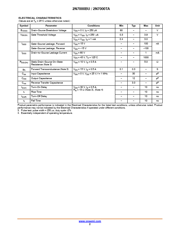
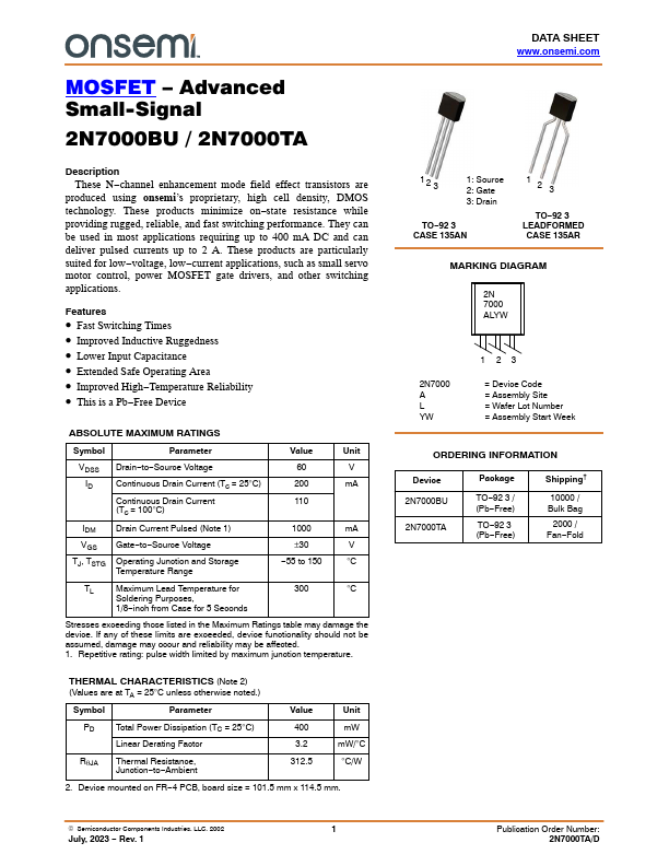
This is a Pb−Free Device ABSOLUTE MAXIMUM RATINGS Symbol Parameter Value Unit VDSS Drain−to−Source Voltage 60 V ID Continuous Drain Current (TC = 25°C) 200 mA Continuous Drain Current 110 (TC = 100°C) IDM VGS TJ, TSTG Drain Current Pulsed (Note 1) Gate−to−Source Voltage Operating Junction and Storage Temperature Range 1000 mA ±30 V −55 to 150 °C TL Maximum Lead Temperature for Soldering Purposes, 1/8−inch from Case for 5 Seconds 300 °C Stresses exceeding those listed in the Maximum Ratings table may damage the device.| Part No. | 2N7000BU |
|---|---|
| Datasheet | 2N7000BU Download |
| Manufacturer |  onsemi |
| Description | Advanced Small-Signal MOSFET |
| Buy | Stock & Price |
DESCRIPTION
These N−channel enhancement mode field effect transistors are produced using onsemi’s proprietary, high cell density, DMOS technology. These products minimize on−state resistance while providing rugged, reliable, and fast switching performance. They can be used in most applications requiring up to 400 mA DC and can deliver pulsed currents up to 2 A. These products are particularly suited for low−voltage, low−current applications, such as small servo motor control, power MOSFET gate drivers, and other switching applications.FEATURES
● Fast Switching Times● Improved Inductive Ruggedness
● Lower Input Capacitance
● Extended Safe Operating Area
● Improved High−Temperature Reliability
● If any of these limits are exceeded, device functionality should not be assumed, damage may occur and reliability may be affected. 1. Repetitive rating: pulse width limited by maximum junction temperature. THERMAL CHARACTERISTICS (Note 2) (Values are at TA = 25°C unless otherwise noted.) Symbol Parameter Value Unit PD Total Power Dissipation (TC = 25°C) Linear Derating Factor 400 mW 3.2 mW/°C RqJA Thermal Resistance, Junction−to−Ambient 312.