onsemi 2SA2112
Bipolar Transistor
| Part No. | 2SA2112 |
|---|---|
| Datasheet | 2SA2112 Download |
| Manufacturer |  onsemi |
| Description | Bipolar Transistor |
| Buy | Stock & Price |
FEATURES
● Adoption of MBIT process● Low collector-to-emitter saturation voltage
● Large current capacity
● High-speed switching Specifications
ABSOLUTE MAXIMUM RATINGS
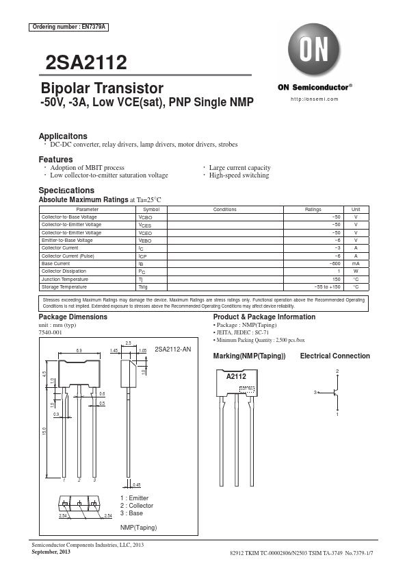
at Ta=25°C Parameter Symbol Collector-to-Base Voltage Collector-to-Emitter Voltage Collector-to-Emitter Voltage Emitter-to-Base Voltage Collector Current Collector Current (Pulse) Base Current Collector Dissipation Junction Temperature VCBO VCES VCEO VEBO IC ICP IB PC Tj Storage Temperature Tstg Conditions Ratings --50 --50 --50 --6 --3 --6 --600 1 150 --55 to +150 Unit V V V V A A mA W °C °C Stresses exceedingMAXIMUM RATINGS
may damage the device.MAXIMUM RATINGS
are stress ratings only. Functional operation above the Recommended Operating Conditions is not implied. Extended exposure to stresses above the Recommended Operating Conditions may affect device reliability. Package Dimensions unit : mm (typ) 7540-001 2.5 6.9 1.45 1.05 2SA2112-AN Product & Package Information● Package : NMP(Taping)
● JEITA, JEDEC : SC-71
● Minimum Packing Quantity : 2,500 pcs./box Marking(NMP(Taping)) Electrical Connection 0.6 0.5 0.9 A2112 LOT No.