onsemi 2SB1302
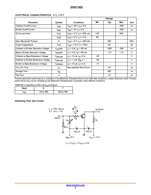
2SB1302 is classified by 500 mA hFE as follows : Rank S T hFE 140 to 280 200 to 400 Switching Time Test Circuit IB1 PW = 20 ms D.C.| Part No. | 2SB1302 |
|---|---|
| Datasheet | 2SB1302 Download |
| Manufacturer |  onsemi |
| Description | Bipolar Transistor |
| Buy | Stock & Price |
FEATURES
● Adoption of FBET, MBIT Processes● Large Current Capacity
● Ultrasmall Size Making it Easy to Provide High−Density Small−Sized Hybrid IC’s
● Low Collector to Emitter Saturation Voltage
● Fast Switching Speed
● These Devices are Pb−Free and are RoHS Compliant
APPLICATIONS
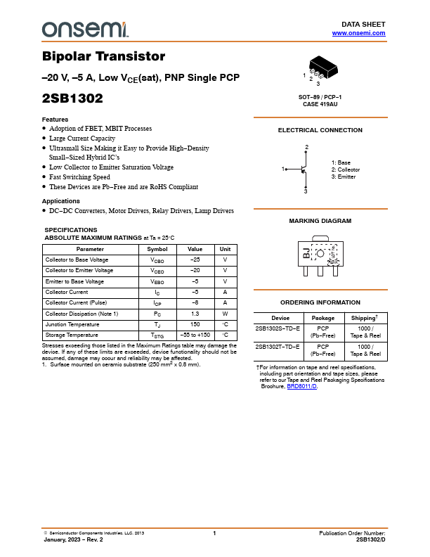
● DC−DC Converters, Motor Drivers, Relay Drivers, Lamp Drivers SPECIFICATIONSABSOLUTE MAXIMUM RATINGS
at Ta = 25°C Parameter Symbol Value Unit Collector to Base Voltage VCBO −25 V Collector to Emitter Voltage VCEO −20 V Emitter to Base Voltage VEBO −5 V Collector Current IC −5 A Collector Current (Pulse) ICP −8 A Collector Dissipation (Note 1) PC 1.3 W Junction Temperature TJ 150 °C Storage Temperature TSTG −55 to +150 °C Stresses exceeding those listed in theMAXIMUM RATINGS
table may damage the device. If any of these limits are exceeded, device functionality should not be assumed, damage may occur and reliability may be affected. 1. Surface mounted on ceramic substrate (250 mm2 x 0.8 mm). 1 2 3 SOT−89 / PCP−1 CASE 419AU ELECTRICAL CONNECTION 2 1 3 1: Base 2: Collector 3: Emitter MARKING DIAGRAM BJ LOT No.