onsemi 2SK545
N-Channel JFET
| Part No. | 2SK545 |
|---|---|
| Datasheet | 2SK545 Download |
| Manufacturer |  onsemi |
| Description | N-Channel JFET |
| Buy | Stock & Price |
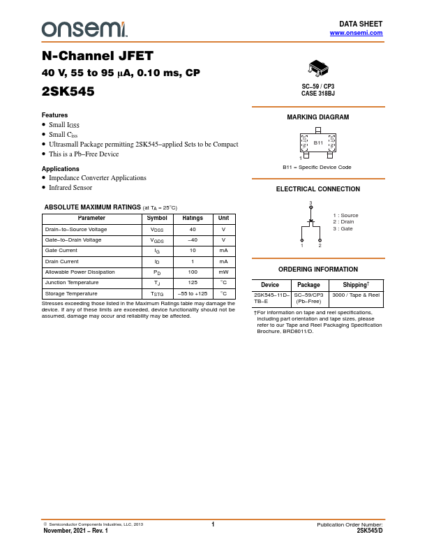
FEATURES
● Small IGSS● Small Ciss
● Ultrasmall Package permitting 2SK545−applied Sets to be Compact
● This is a Pb−Free Device
APPLICATIONS
● Impedance ConverterAPPLICATIONS
● Infrared SensorABSOLUTE MAXIMUM RATINGS
(at TA = 25°C) Parameter Symbol Ratings Unit Drain−to−Source Voltage VDSS 40 V Gate−to−Drain Voltage VGDS −40 V Gate Current IG 10 mA Drain Current ID 1 mA Allowable Power Dissipation PD 100 mW Junction Temperature TJ 125 °C Storage Temperature TSTG −55 to +125 °C Stresses exceeding those listed in theMAXIMUM RATINGS
table may damage the device. If any of these limits are exceeded, device functionality should not be assumed, damage may occur and reliability may be affected. MARKING DIAGRAM LOT No. LOT No. B11 1 B11 = Specific Device Code ELECTRICAL CONNECTION 3 1 : Source 2 : Drain 3 : Gate 1 2 ORDERING INFORMATION Device Package Shipping† 2SK545−11D− SC−59/CP3 3000 / Tape & Reel TB−E (Pb−Free) †For information on tape and reel specifications, including part orientation...