onsemi 3LN01M
the 3LN01M is a MOSFET product, please avoid using this device in the vicinity of highly charged objects.| Part No. | 3LN01M |
|---|---|
| Datasheet | 3LN01M Download |
| Manufacturer |  onsemi |
| Description | Small Signal MOSFET |
| Buy | Stock & Price |
FEATURES
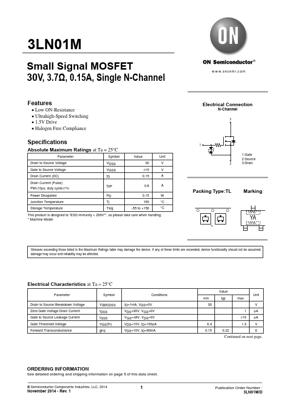
● Low ON-Resistance● Ultrahigh-Speed Switching
● 1.5V Drive
● Halogen Free Compliance Specifications
ABSOLUTE MAXIMUM RATINGS
at Ta = 25°C Parameter Symbol Value Unit Drain to Source Voltage Gate to Source Voltage Drain Current (DC) VDSS VGSS ID 30 ±10 0.15 V V A Drain Current (Pulse) PW≤10μs, duty cycle≤1% IDP 0.6 A Power Disspation Junction Temperature Storage Temperature PD 0.15 W Tj 150 °C Tstg −55 to +150 °C This product is designed to “ESD immunity < 200V*”, so please take care when handling. * Machine Model Electrical Connection N-Channel 3 1 1:Gate 2:Source 2 3:Drain Packing Type:TL Marking LOT No. YA LOT No. TL Stresses exceeding those listed in theMAXIMUM RATINGS
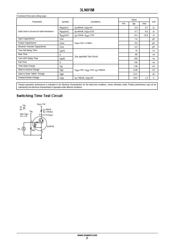
table may damage the device. If any of these limits are exceeded, device functionality should not be assumed, damage may occur and reliability may be affected.ELECTRICAL CHARACTERISTICS
at Ta = 25°C Parameter Symbol Drain to Source Breakdown Voltage Zero-Gate Voltage Drain Current Gate to Source Leakage C...