onsemi 74AC14
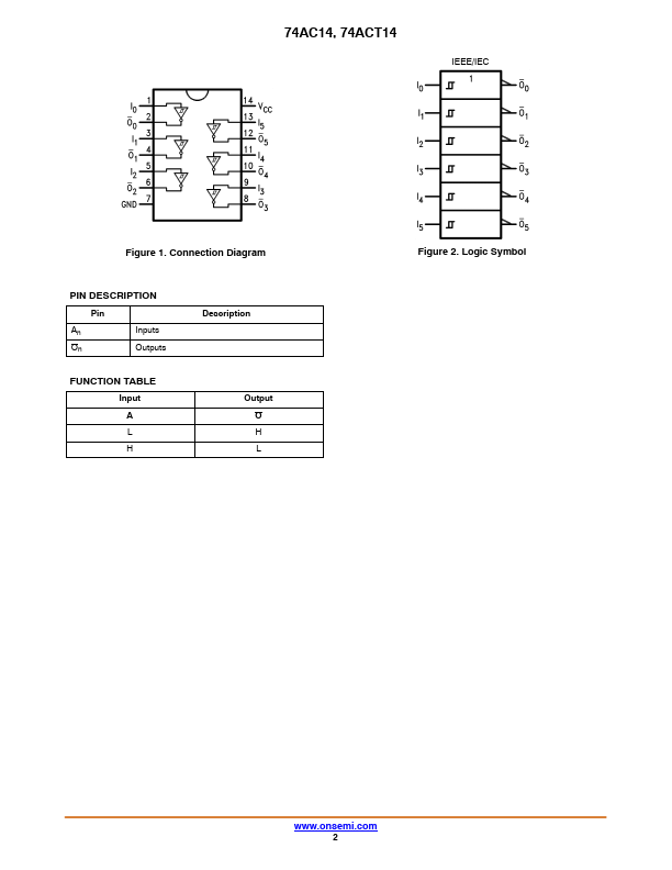
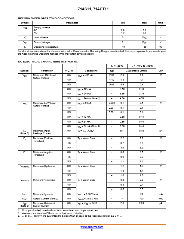
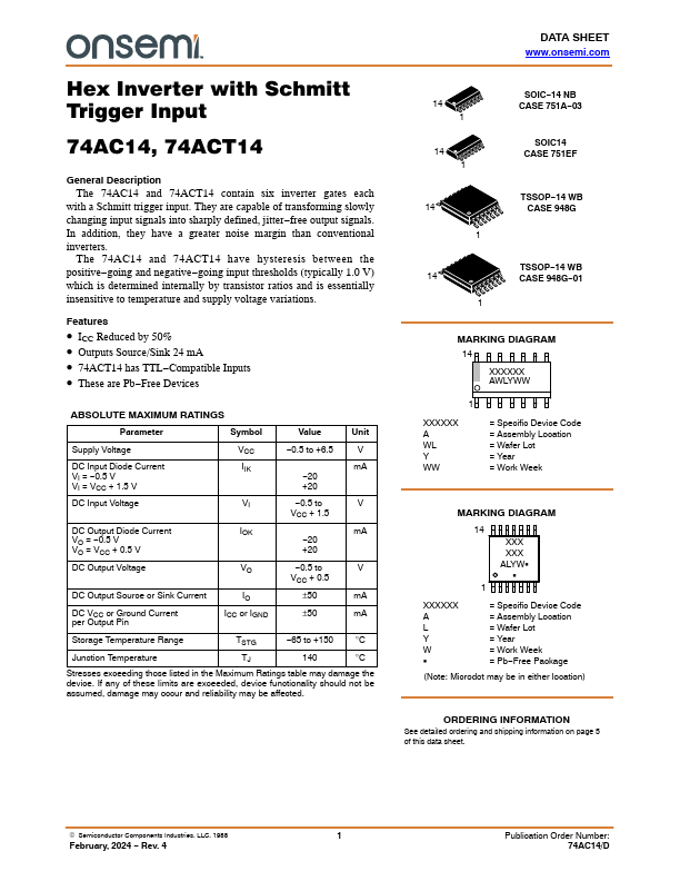
The 74AC14 and 74ACT14 contain six inverter gates each with a Schmitt trigger input. They are capable of transforming slowly changing input signals into sharply defined, jitter−free output signals. The 74AC14 and 74ACT14 have hysteresis between the positive−going and negative−going input thresholds (typically 1.0 V) which is determined internally by transistor ratios and is essentially insensitive to temperature and supply voltage variations.| Part No. | 74AC14 |
|---|---|
| Datasheet | 74AC14 Download |
| Manufacturer |  onsemi |
| Description | Hex Inverter |
| Buy | Stock & Price |
GENERAL DESCRIPTION
In addition, they have a greater noise margin than conventional inverters.FEATURES
● ICC Reduced by 50%● Outputs Source/Sink 24 mA
● 74ACT14 has TTL−Compatible Inputs
● These are Pb−Free Devices
ABSOLUTE MAXIMUM RATINGS
Parameter Symbol Value Unit Supply Voltage VCC −0.5 to +6.5 V DC Input Diode Current VI = −0.5 V VI = VCC + 1.5 V IIK mA −20 +20 DC Input Voltage VI −0.5 to V VCC + 1.5 DC Output Diode Current VO = −0.5 V VO = VCC + 0.5 V IOK mA −20 +20 DC Output Voltage VO −0.5 to V VCC + 0.5 DC Output Source or Sink Current IO ±50 mA DC VCC or Ground Current per Output Pin ICC or IGND ±50 mA Storage Temperature Range TSTG −65 to +150 °C Junction Temperature TJ 140 °C Stresses exceeding those listed in theMAXIMUM RATINGS
table may damage the device. If any of these limits are exceeded, device functionality should not be assumed, damage may occur and reliability may be affected. DATA SHEET 14 1 14 1 14 1 14 1 SOIC−14 NB CASE 751A−03 SOIC14 CASE 751EF TSSOP−14 WB C...