onsemi 74ACT374
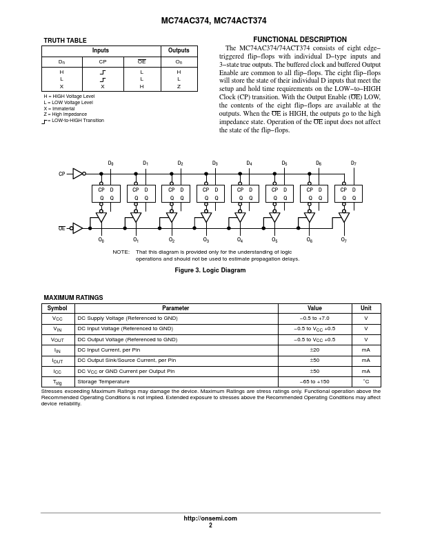
The MC74AC374/74ACT374 consists of eight edge− triggered flip−flops with individual D−type inputs and 3−state true outputs. The buffered clock and buffered Output Enable are common to all flip−flops.| Part No. | 74ACT374 |
|---|---|
| Datasheet | 74ACT374 Download |
| Manufacturer |  onsemi |
| Description | OCTAL D-TYPE FLIP-FLOP |
| Buy | Stock & Price |
FEATURES
●●
●
●
●
●
●
●
●
● Buffered Positive Edge−Triggered Clock 3−State Outputs for Bus−Oriented
APPLICATIONS
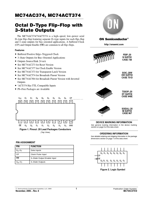
Outputs Source/Sink 24 mA See MC74AC273 for Reset Version See MC74AC377 for Clock Enable Version See MC74AC373 for Transparent Latch Version See MC74AC574 for Broadside Pinout Version See MC74AC564 for Broadside Pinout Version with Inverted Outputs ′ACT374 Has TTL Compatible Inputs Pb−Free Packages are Available PDIP−20 N SUFFIX CASE 738 1 SOIC−20W DW SUFFIX CASE 751D 1 VCC 20 O7 19 D7 18 D6 17 O6 16 O5 15 D5 14 D4 13 O4 12 CP 11 TSSOP−20 DT SUFFIX CASE 948E 1 SOEIAJ−20 M SUFFIX CASE 967 1 1 OE 2 O0 3 D0 4 D1 5 O1 6 O2 7 D2 8 D3 9 O3 10 GND DEVICE MARKING INFORMATION See general marking information in the device marking section on page 6 of this data sheet. Figure 1. Pinout: 20 Lead Packages Conductors (Top View) ORDERING INFORMATION See detailed ordering and shipping information in the package dimensions section on page 7 of this data sheet. PIN ASSIGNMENT PIN D0−D7 CP OE...