onsemi 74ALVC16244
The 74ALVC16244 is designed for low voltage (1.65 V to 3.6 V) VCC applications with I/O capability up to 3.6 V. The 74ALVC16244 is fabricated with an advanced CMOS technology to achieve high speed operation while maintaining low CMOS power dissipation. Pin Assignment for TSSOP PIN DESCRIPTION Pin Names Description OEn I0−I15 O0−O15 NC Output Enable Input (Active LOW) Inputs Outputs No Connect OE4 I12−I15 O12−O15 L L L L H H H X Z H = HIGH Voltage Level L = LOW Voltage Level X = Immaterial (HIGH or LOW, inputs may not float) Z = High Impedance...| Part No. | 74ALVC16244 |
|---|---|
| Datasheet | 74ALVC16244 Download |
| Manufacturer |  onsemi |
| Description | Low-Voltage 16-Bit Buffer/Line Driver |
| Buy | Stock & Price |
GENERAL DESCRIPTION
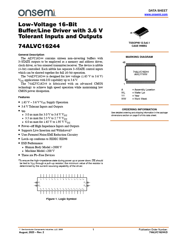
The ALVC16244 contains sixteen non−inverting buffers with 3−STATE outputs to be employed as a memory and address driver, clock driver, or bus oriented transmitter/receiver. The device is nibble (4−bit) controlled. Each nibble has separate 3−STATE control inputs which can be shorted together for full 16−bit operation.FEATURES
● 1.65 V − 3.6 V VCC Supply Operation● 3.6 V Tolerant Inputs and Outputs
● tPD ♦ 3.0 ns max for 3.0 V to 3.6 V VCC ♦ 3.5 ns max for 2.3 V to 2.7 V VCC ♦ 6.0 ns max for 1.65 V to 1.95 V VCC
● Power−off High Impedance Inputs and Outputs
● Supports Live Insertion and Withdrawal*
● Uses Patented Noise/EMI Reduction Circuitry
● Latch−up conforms to JEDEC JED98
● ESD Performance: ♦ Human Body Model >2000 V ♦ Machine Model >200 V
● These are Pb−Free Devices *To ensure the high−impedance state during power up or power down, OE should be tied to VCC through a pull−up resistor; the minimum value of the resistor is determined by the current−sourcing capability of the driver.

