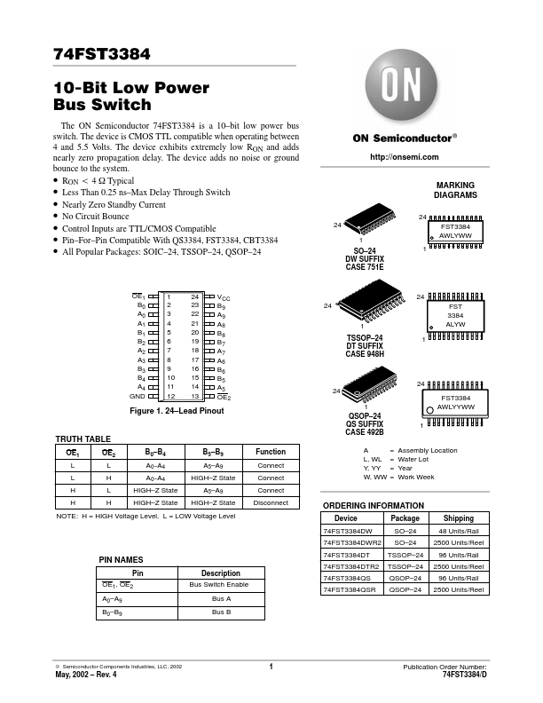
DESCRIPTION
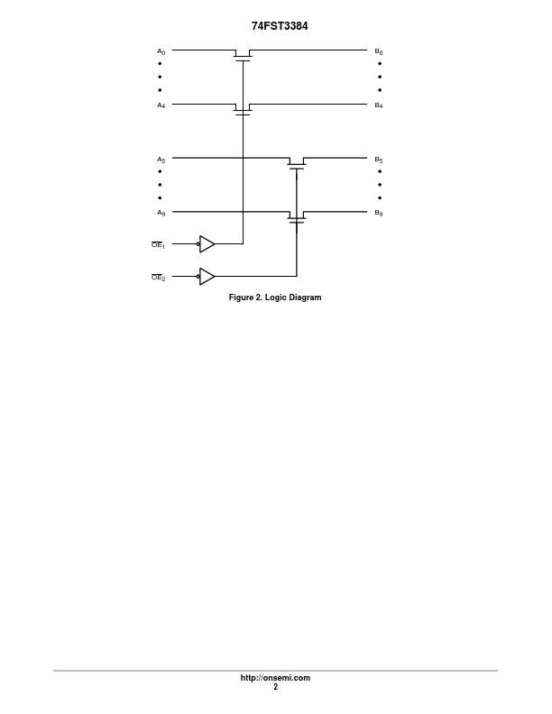
Bus Switch Enable Bus A Bus B 74FST3384QS 74FST3384QSR © Semiconductor Components Industries, LLC, 2002 1 May, 2002 – Rev. 4 Publication Order Number: 74FST3384/D 74FST3384 A0 B0 A4 B4 A5 B5 A9 B9 OE1 OE2 Figure 2. Logic Diagram 2 74FST3384 MAXIMUM RATINGS
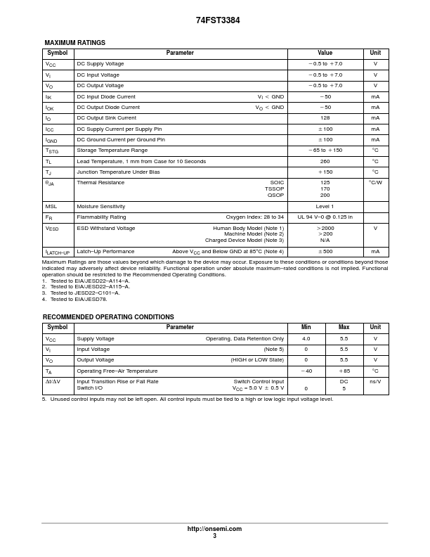
Symbol VCC VI VO IIK IOK IO ICC IGND TSTG TL TJ qJA DC Supply Voltage DC Input Voltage DC Output Voltage DC Input Diode Current DC Output Diode Current DC Output Sink Current DC Supply Current per Supply Pin DC Ground Current per Ground Pin Storage Temperature Range Lead Temperature, 1 mm from Case for 10 Seconds Junction Temperature Under Bias Thermal Resistance SOIC TSSOP QSOP VI t GND VO t GND Parameter Value *0.5 to )7.0 *0.5 to )7.0 *0.5 to )7.0 *50 *50 128 $100 $100 *65 to )150 260 )150 125 170 200 Level 1 Oxygen Index: 28 to 34 Human Body Model (Note 1) Machine Model (Note 2) Charged Device Model (Note 3) Above VCC and Below GND at 85°C (Note 4) UL 94 V–0 @ 0.125 in u2000 u200 N/A $500 V Unit V V V mA mA mA mA mA °... onsemi