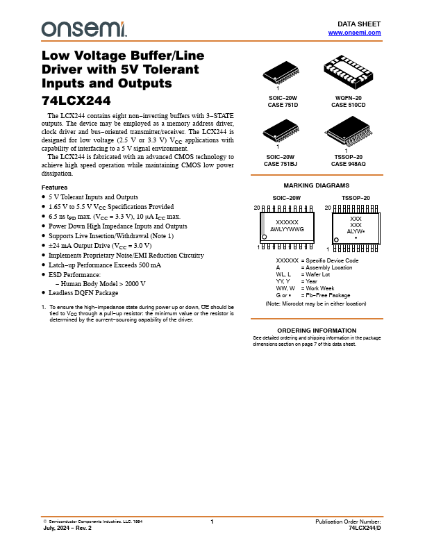
Datasheet4U Logo Datasheet4U.com

74LCX244 - Low Voltage Buffer/Line Driver

General Description

Pin Names OE1, OE2 I0 I7 O0

2.

STATE Output Enable Inputs Inputs Outputs No Connect O0 O1 O2 O3 O4 O5 O6 O7 Outputs (Pins 12, 14, 16, 18) L H Z Outputs (Pins 3, 5, 7, 9) L H Z www.onsemi.com 2 74LCX244 MAXIMUM RATINGS Symbol Pa

Key Features

  • 5 V Tolerant Inputs and Outputs.
  • 1.65 V to 5.5 V VCC Specifications Provided.
  • 6.5 ns tPD max. (VCC = 3.3 V), 10 mA ICC max.
  • Power Down High Impedance Inputs and Outputs.
  • Supports Live Insertion/Withdrawal (Note 1).
  • ±24 mA Output Drive (VCC = 3.0 V).
  • Implements Proprietary Noise/EMI Reduction Circuitry.
  • Latch.
  • up Performance Exceeds 500 mA.
  • ESD Performance:.
  • Human Body Model > 2000 V.
  • Leadl.

📥 Download Datasheet

Datasheet Details

Part number 74LCX244
Manufacturer onsemi
File Size 169.95 KB
Description Low Voltage Buffer/Line Driver
Datasheet download datasheet 74LCX244 Datasheet

Full PDF Text Transcription (Reference)

The following content is an automatically extracted verbatim text from the original manufacturer datasheet and is provided for reference purposes only.

View original datasheet text
Low Voltage Buffer/Line Driver with 5V Tolerant Inputs and Outputs 74LCX244 The LCX244 contains eight non−inverting buffers with 3−STATE outputs. The device may be employed as a memory address driver, clock driver and bus−oriented transmitter/receiver. The LCX244 is designed for low voltage (2.5 V or 3.3 V) VCC applications with capability of interfacing to a 5 V signal environment. The LCX244 is fabricated with an advanced CMOS technology to achieve high speed operation while maintaining CMOS low power dissipation. Features • 5 V Tolerant Inputs and Outputs • 1.65 V to 5.5 V VCC Specifications Provided • 6.5 ns tPD max. (VCC = 3.3 V), 10 mA ICC max. • Power Down High Impedance Inputs and Outputs • Supports Live Insertion/Withdrawal (Note 1) • ±24 mA Output Drive (VCC = 3.