DESCRIPTION
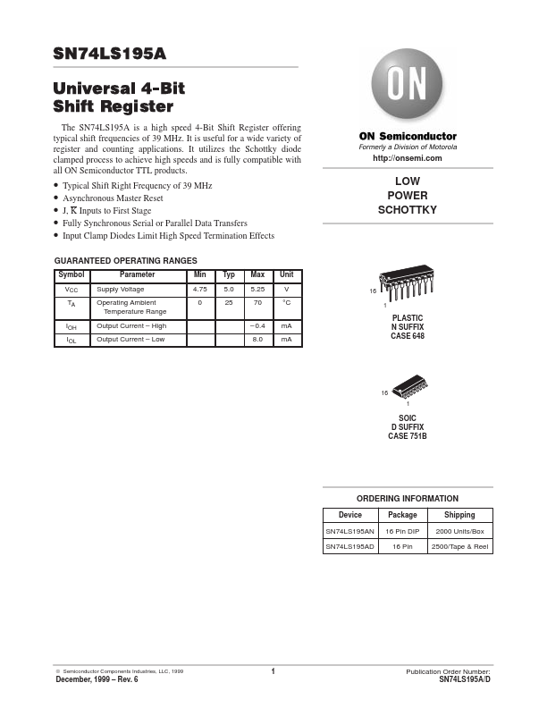
It performs serial, parallel, serial to parallel, or parallel to serial data transfers at very high speeds. The LS195A has two primary modes of operation, shift right (Q0 Q1) and parallel load which are controlled by the state of the Parallel Enable (PE) input. When the PE input is HIGH, serial data enters the first flip-flop Q0 via the J and K inputs and is shifted one bit in the direction Q0 Q1 Q2 Q3 following each LOW to HIGH clock transition. The JK inputs provide the flexibility of the JK type input for special applications, and the simple D type input for general applications by tying the two pins together. When the PE ³ ³ ³ ³ input is LOW, the LS195A appears as four common clocked D flip-flops. The data on the parallel inputs P0, P1, P2, P3 is transferred to the respective Q0, Q1, Q2, Q3 outputs following the LOW to HIGH clock transition. Shift left operations (Q3 Q2) can be achieved by tying the Qn Outputs to the Pn–1 inputs and holding the PE input LOW. All serial and parallel data transfers are synchronous, occurring after each LOW to HIGH clock transition. onsemi