FEATURES
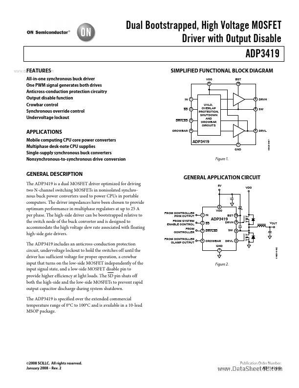
SIMPLIFIED FUNCTIONAL BLOCK DIAGRAM VCC 5 All-in-one synchronous buck driver One PWM signal generates both drives Anticross-conduction protection circuitry Output disable function Crowbar control Synchronous override control Undervoltage lockout BST 10 IN 1 SD 2 UVLO, OVERLAP PROTECTION, SHUTDOWN AND CROWBAR CIRCUITS 9 DRVH SW 8 DRVLSD 3 CROWBAR 4 APPLICATIONS
Mobile computing CPU core power converters Multiphase desk-note CPU supplies Single-supply synchronous buck converters Nonsynchronous-to-synchronous drive conversion 6 DRVL 04620-0-001 ADP3419 7 GND Figure 1. GENERAL DESCRIPTION
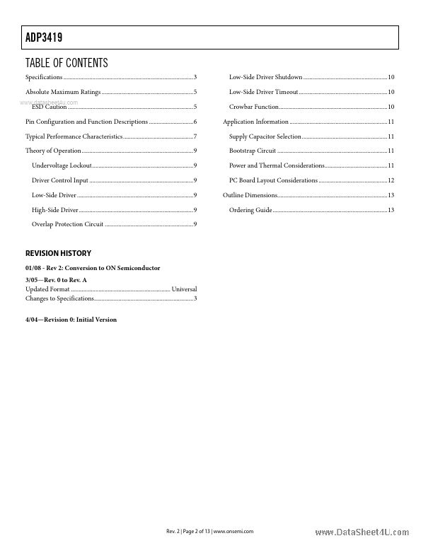
The ADP3419 includes an anticross-conduction protection circuit, undervoltage lockout to hold the switches off until the driver has sufficient voltage for proper operation, a crowbar input that turns on the low-side MOSFET independently of the input signal state, and a low-side MOSFET disable pin to provide higher efficiency at light loads. The SD pin shuts off both the high-side and the low-side MOSFETs to prevent rapid output capacitor discharge during system shutdown. onsemi