onsemi ATP108
P-Channel Power MOSFET
| Part No. | ATP108 |
|---|---|
| Datasheet | ATP108 Download |
| Manufacturer |  onsemi |
| Description | P-Channel Power MOSFET |
| Buy | Stock & Price |
FEATURES
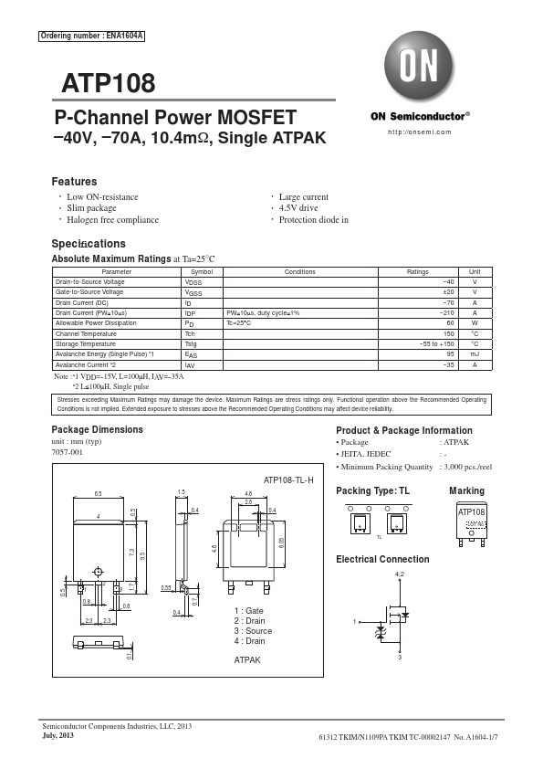
● Low ON-resistance● Slim package
● Halogen free compliance
● Large current
● 4.5V drive
● Protection diode in Specifications
ABSOLUTE MAXIMUM RATINGS
at Ta=25°C Parameter Symbol Drain-to-Source Voltage Gate-to-Source Voltage Drain Current (DC) Drain Current (PW≤10μs) Allowable Power Dissipation Channel Temperature VDSS VGSS ID IDP PD Tch Storage Temperature Tstg Avalanche Energy (Single Pulse) *1 EAS Avalanche Current *2 IAV Note :*1 VDD=--15V, L=100μH, IAV=--35A *2 L≤100μH, Single pulse Conditions PW≤10μs, duty cycle≤1% Tc=25°C Ratings --40 ±20 --70 --210 60 150 --55 to +150 95 --35 Unit V V A A W °C °C mJ A Stresses exceedingMAXIMUM RATINGS
may damage the device.MAXIMUM RATINGS
are stress ratings only. Functional operation above the Recommended Operating Conditions is not implied. Extended exposure to stresses