onsemi BAW56LT1
Monolithic Dual Switching Diode Common Anode
| Part No. | BAW56LT1 |
|---|---|
| Datasheet | BAW56LT1 Download |
| Manufacturer |  onsemi |
| Description | Monolithic Dual Switching Diode Common Anode |
| Buy | Stock & Price |
FEATURES
● Pb−Free Packages are AvailableMAXIMUM RATINGS
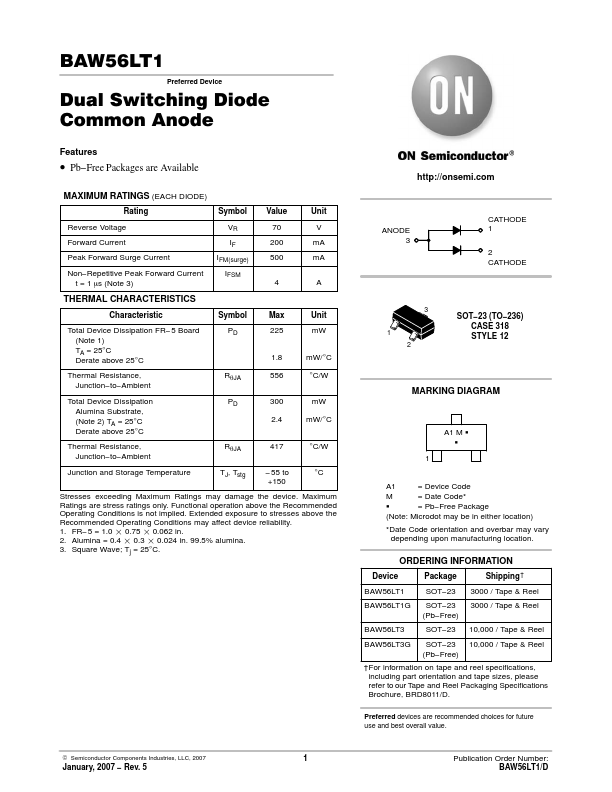
(EACH DIODE) Rating Reverse Voltage Forward Current Peak Forward Surge Current Non−Repetitive Peak Forward Current t = 1 ms (Note 3) Symbol VR IF IFM(surge) IFSM 4 A Value 70 200 500 Unit V mA mA ANODE 3 CATHODE 1 2 CATHODE THERMAL CHARACTERISTICS Characteristic Total Device Dissipation FR− 5 Board (Note 1) TA = 25°C Derate above 25°C Thermal Resistance, Junction−to−Ambient Total Device Dissipation Alumina Substrate, (Note 2) TA = 25°C Derate above 25°C Thermal Resistance, Junction−to−Ambient Junction and Storage Temperature Symbol PD Max 225 1.8 RqJA PD 556 300 2.4 417 −55 to +150 Unit mW mW/°C °C/W 1 2 3 SOT−23 (TO−236) CASE 318 STYLE 12 MARKING DIAGRAM mW mW/°C °C/W 1 TJ, Tstg °C A1 = Device Code M = Date Code* G = Pb−Free Package (Note: Microdot may be in either location) *Date Code orientation and overbar may vary depending upon manufacturing location. A1 M G G RqJA Stresses exceedingMAXIMUM RATINGS
may damage the device.MAXIMUM RATINGS
are stress ratings only.