onsemi BC327
PNP Epitaxial Silicon Transistor
| Part No. | BC327 |
|---|---|
| Datasheet | BC327 Download |
| Manufacturer |  onsemi |
| Description | PNP Epitaxial Silicon Transistor |
| Buy | Stock & Price |
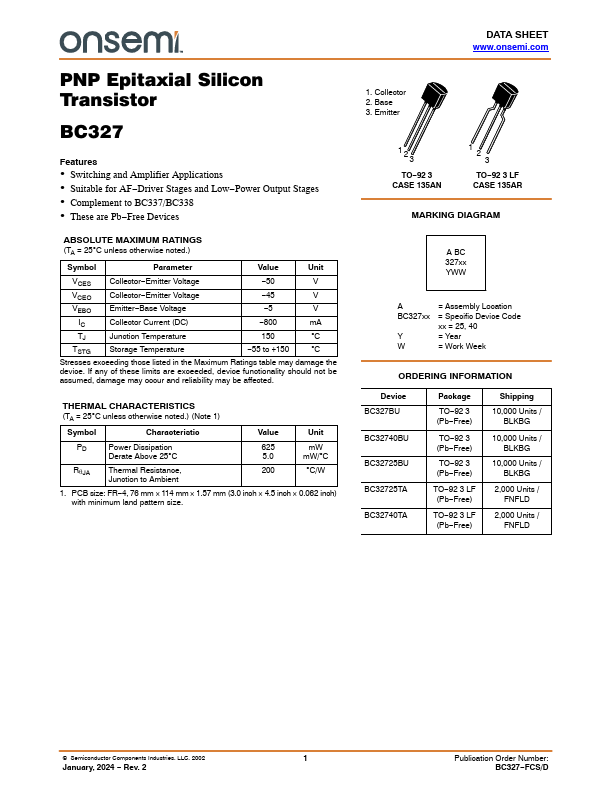
FEATURES
● Switching and AmplifierAPPLICATIONS
● Suitable for AF−Driver Stages and Low−Power Output Stages● Complement to BC337/BC338
● These are Pb−Free Devices
ABSOLUTE MAXIMUM RATINGS
(TA = 25C unless otherwise noted.) Symbol Parameter Value Unit VCES Collector−Emitter Voltage −50 V VCEO Collector−Emitter Voltage −45 V VEBO Emitter−Base Voltage −5 V IC Collector Current (DC) −800 mA TJ Junction Temperature 150 C TSTG Storage Temperature −55 to +150 C Stresses exceeding those listed in theMAXIMUM RATINGS
table may damage the device. If any of these limits are exceeded, device functionality should not be assumed, damage may occur and reliability may be affected. THERMAL CHARACTERISTICS (TA = 25C unless otherwise noted.) (Note 1) Symbol Characteristic Value Unit PD Power Dissipation Derate Above 25C 625 mW 5.0 mW/C RqJA Thermal Resistance, Junction to Ambient 200 C/W 1. PCB size: FR−4, 76 mm 114 mm 1.57 mm (3.0 inch 4.5 inch 0.062 inch) with minimum land pattern size. DATA SHEET 1.