onsemi BC859CLT1G
General Purpose Transistors
| Part No. | BC859CLT1G |
|---|---|
| Datasheet | BC859CLT1G Download |
| Manufacturer |  onsemi |
| Description | General Purpose Transistors |
| Buy | Stock & Price |
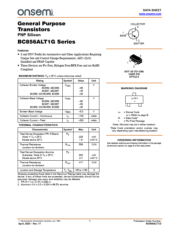
FEATURES
● S and NSV Prefix for Automotive and OtherAPPLICATIONS
Requiring Unique Site and Control Change Requirements; AEC−Q101 Qualified and PPAP Capable● These Devices are Pb−Free, Halogen Free/BFR Free and are RoHS Compliant
MAXIMUM RATINGS
(TA = 25°C unless otherwise noted) Rating Symbol Value Unit Collector-Emitter Voltage VCEO V BC856, SBC856 −65 BC857, SBC857 −45 BC858, NSVBC858, BC859 −30 Collector-Base Voltage VCBO V BC856, SBC856 −80 BC857, SBC857 −50 BC858, NSVBC858, BC859 −30 Emitter−Base Voltage Collector Current − Continuous Collector Current − Peak THERMAL CHARACTERISTICS VEBO IC IC −5.0 −100 −200 V mAdc mAdc Characteristic Symbol Max Unit Total Device Dissipation FR− 5 Board, PD (Note 1) TA = 25°C Derate above 25°C 225 mW 1.8 mW/°C Thermal Resistance, Junction−to−Ambient RqJA 556 °C/W Total Device Dissipation Alumina Substrate, (Note 2) TA = 25°C Derate above 25°C PD 300 mW 2.4 mW/°C Thermal Resistance, Junction−to−Ambient RqJA 417 °C/W Junction and Storage Temperature TJ, Tstg − 55 to +150 °C Stresses exceeding those listed in theMAXIMUM RATINGS
table may damage the device.