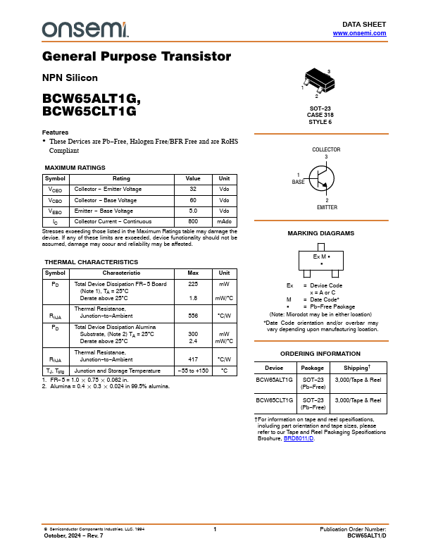
BCW65ALT1G
Features
- These Devices are Pb- Free, Halogen Free/BFR Free and are Ro HS pliant
MAXIMUM RATINGS
Symbol
Rating
Value
Unit
VCEO Collector
- Emitter Voltage
Vdc
VCBO Collector
- Base Voltage
Vdc
VEBO Emitter
- Base Voltage
Vdc
Collector Current
- Continuous
800 m Adc
Stresses exceeding those listed in the Maximum Ratings table may damage the device. If any of these limits are exceeded, device functionality should not be assumed, damage may occur and reliability may be affected.
THERMAL CHARACTERISTICS
Symbol
Characteristic
Total Device Dissipation FR- 5 Board
(Note 1), TA = 25C
Derate above 25C
Rq JA PD
Thermal Resistance, Junction- to- Ambient
Total Device Dissipation Alumina Substrate, (Note 2) TA = 25C Derate above 25C
Rq JA
Thermal Resistance, Junction- to- Ambient
TJ, Tstg Junction and Storage Temperature
1. FR- 5 = 1.0 0.75 0.062 in. 2. Alumina = 0.4 0.3 0.024 in 99.5% alumina.
Max 225...