onsemi D45C12
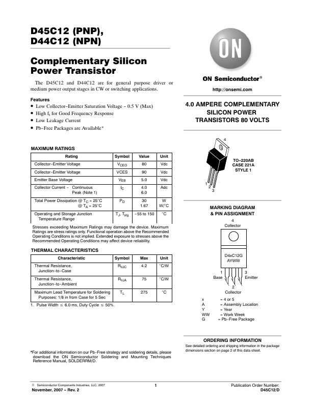
The D45C12 and D44C12 areĂfor general purpose driver or medium power output stages in CW or switching applications.| Part No. | D45C12 |
|---|---|
| Datasheet | D45C12 Download |
| Manufacturer |  onsemi |
| Description | Complementary Silicon Power Transistor |
| Buy | Stock & Price |
FEATURES
●ăLow Collector-Emitter Saturation Voltage - 0.5 V (Max)●ăHigh ft for Good Frequency Response
●ăLow Leakage Current
●ăPb-Free Packages are Available* ÎÎÎÎÎÎÎÎÎÎÎÎÎÎÎÎÎÎÎMAXIMUM RATINGS ÎÎÎÎÎÎÎÎÎÎÎÎÎÎÎÎÎÎÎRating Symbol Value Unit ÎÎÎÎÎÎÎÎÎÎÎÎÎÎÎÎÎÎÎCollector-Emitter Voltage ÎÎÎÎÎÎÎÎÎÎÎÎÎÎÎÎÎÎÎCollector-Emitter Voltage VCEO 80 Vdc VCES 90 Vdc ÎÎÎÎÎÎÎÎÎÎÎÎÎÎÎÎÎÎÎEmitter Base Voltage ÎÎÎÎÎÎÎÎÎÎÎÎÎÎÎÎÎÎÎCollector Current - Continuous Peak (Note 1) VEB 5.0 Vdc IC 4.0 Adc 6.0 ÎÎÎÎÎÎÎÎÎÎÎÎÎÎÎÎÎÎÎÎÎÎÎÎÎÎÎÎÎÎÎÎÎÎÎÎÎÎTotal Power Dissipation @ TC = 25°C Total Power Dissipation @ TA = 25°C ÎÎÎÎÎÎÎÎÎÎÎÎÎÎÎÎÎÎÎOperating and Storage Junction ÎÎÎÎÎÎÎÎÎÎÎÎÎÎÎÎÎÎÎTemperature Range PD TJ, Tstg 30 1.67 -ā55 to 150 W W/°C °C ÎÎÎÎÎÎÎÎÎÎÎÎÎÎÎÎÎÎÎStresses exceeding
MAXIMUM RATINGS
may damage the device.MAXIMUM RATINGS
are stress ratings only. Functional operation above the Recommended ÎÎÎÎÎÎÎÎÎÎÎÎÎÎÎÎÎÎÎOperating Conditions is not implied. Extended exposure to stresses above the ÎÎÎÎÎÎÎÎÎÎÎÎÎÎÎÎÎÎÎR...
