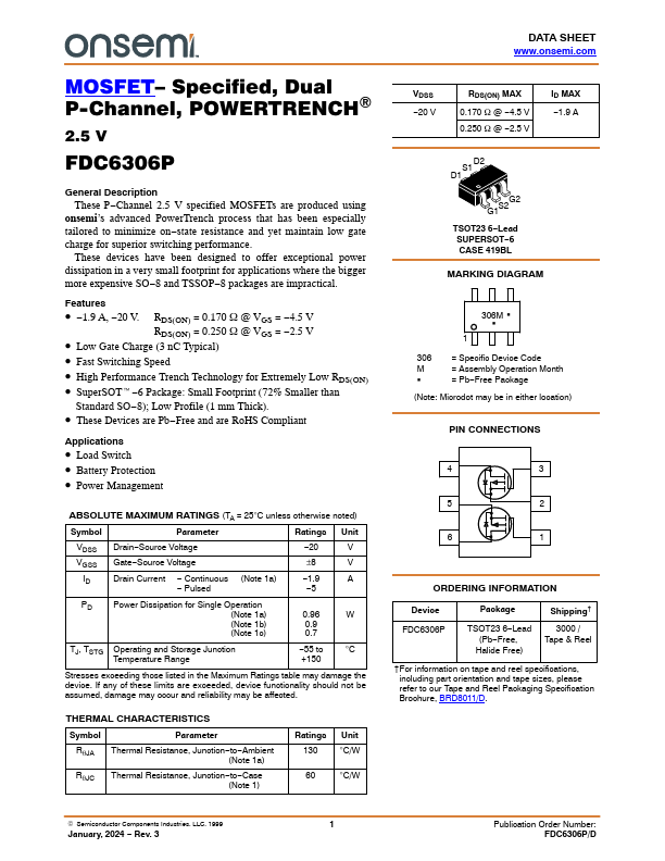
FDC6306P
Description
These P- Channel 2.5 V specified MOSFETs are produced using onsemi’s advanced Power Trench process that has been especially tailored to minimize on- state resistance and yet maintain low gate charge for superior switching performance.
These devices have been designed to offer exceptional power dissipation in a very small footprint for applications where the bigger more expensive SO- 8 and TSSOP- 8 packages are impractical.
Features
- - 1.9 A,
- 20 V. RDS(ON) = 0.170 W @ VGS =
- 4.5 V
RDS(ON) = 0.250 W @ VGS =
- 2.5 V
- Low Gate Charge (3 n C Typical)
- Fast Switching Speed
- High Performance Trench Technology for Extremely Low RDS(ON)
- Super SOTt- 6 Package: Small Footprint (72% Smaller than
Standard SO- 8); Low Profile (1 mm Thick).
- These Devices are Pb- Free and are Ro HS pliant
Applications
- Load Switch
- Battery Protection
- Power Management
ABSOLUTE MAXIMUM RATINGS (TA = 25°C unless otherwise noted)
Symbol
Parameter
Ratings Unit
VDSS Drain- Source Voltage
- 20
VGSS Gate-...