GENERAL DESCRIPTION
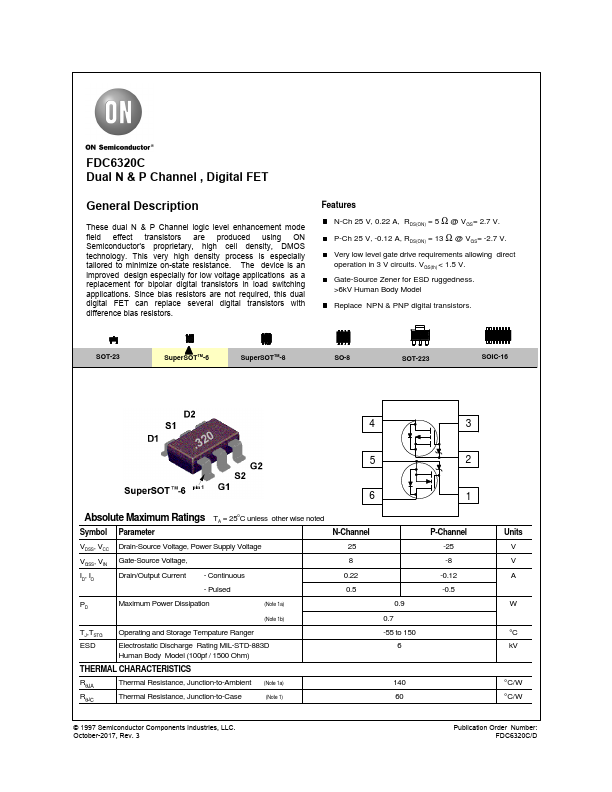
These dual N & P Channel logic level enhancement mode field effect transistors are produced using ON Semiconductor's proprietary, high cell density, DMOS technology. Since bias resistors are not required, this dual digital FET can replace several digital transistors with difference bias resistors. FEATURES
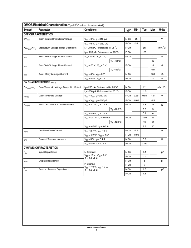
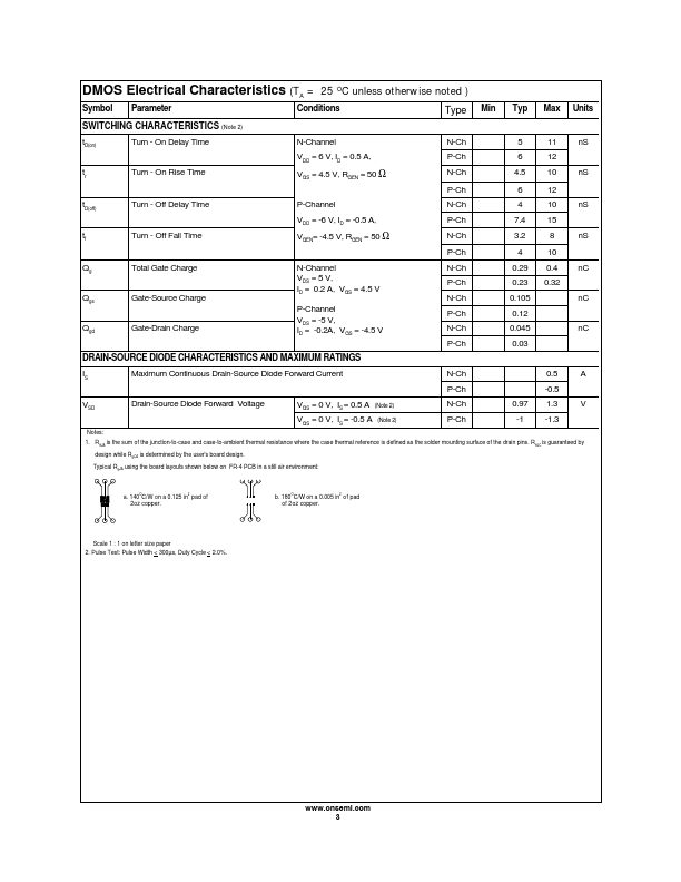
N-Ch 25 V, 0.22 A, RDS(ON) = 5 Ω @ VGS= 2.7 V. P-Ch 25 V, -0.12 A, RDS(ON) = 13 Ω @ VGS= -2.7 V. Very low level gate drive requirements allowing direct operation in 3 V circuits. VGS(th) < 1.5 V. Gate-Source Zener for ESD ruggedness. >6kV Human Body Model Replace NPN & PNP digital transistors. SOT-23 SuperSOTTM-6 SuperSOTTM-8 SO-8 SOT-223 SOIC-16 43 52 61 ABSOLUTE MAXIMUM RATINGS
TA = 25oC unless other wise noted Symbol Parameter N-Channel VDSS, VCC VGSS, VIN ID, IO Drain-Source Voltage, Power Supply Voltage Gate-Source Voltage, Drain/Output Current - Continuous - Pulsed 25 8 0.22 0.5 PD Maximum Power Dissipation (Note 1a) (Note 1b) TJ,TSTG ESD Operating and Stora... onsemi