onsemi FDC6323L
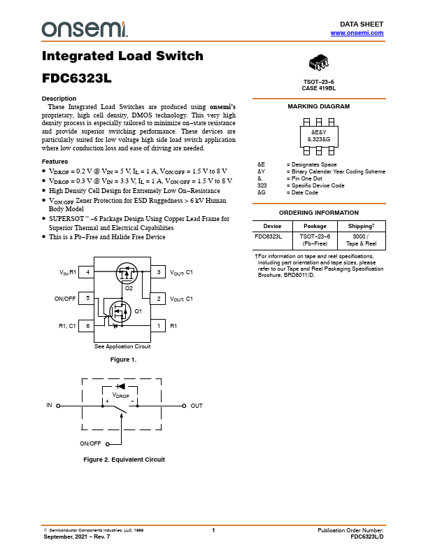
This very high density process is especially tailored to minimize on−state resistance and provide superior switching performance. These devices are particularly suited for low voltage high side load switch application where low conduction loss and ease of driving are needed.| Part No. | FDC6323L |
|---|---|
| Datasheet | FDC6323L Download |
| Manufacturer |  onsemi |
| Description | Integrated Load Switch |
| Buy | Stock & Price |
DESCRIPTION
These Integrated Load Switches are produced using onsemi’s proprietary, high cell density, DMOS technology.FEATURES
● VDROP = 0.2 V @ VIN = 5 V, IL = 1 A, VON/OFF = 1.5 V to 8 V● VDROP = 0.3 V @ VIN = 3.3 V, IL = 1 A, VON/OFF = 1.5 V to 8 V
● High Density Cell Design for Extremely Low On−Resistance
● VON/OFF Zener Protection for ESD Ruggedness > 6 kV Human Body Model
● SUPERSOTt−6 Package Design Using Copper Lead Frame for Superior Thermal and Electrical Capabilities
● This is a Pb−Free and Halide Free Device VIN,R1 4 ON/OFF 5 R1, C1 6 Q2 Q1 3 VOUT, C1 2 VOUT, C1 1 R1 See Application Circuit Figure 1. DATA SHEET TSOT−23−6 CASE 419BL MARKING DIAGRAM &E&Y &.323&G &E = Designates Space &Y = Binary Calendar Year Coding Scheme &. = Pin One Dot 323 = Specific Device Code &G = Date Code ORDERING INFORMATION Device FDC6323L Package TSOT−23−6 (Pb−Free) Shipping† 3000 / Tape & Reel †For information on tape and reel specifications, including part orientation and tape sizes, please refer to our Tape and Reel Packaging Specification Brochure, BRD8011/D.

