onsemi FDC6325L
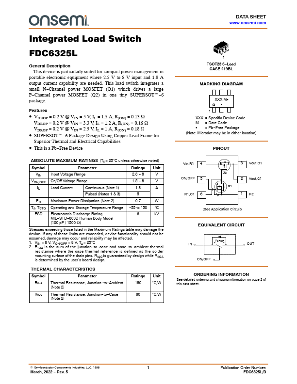
This device is particularly suited for compact power management in portable electronic equipment where 2.5 V to 8 V input and 1.8 A output current capability are needed. This load switch integrates a small N−Channel power MOSFET (Q1) which drives a large P−Channel power MOSFET (Q2) in one tiny SUPERSOTt−6 package.| Part No. | FDC6325L |
|---|---|
| Datasheet | FDC6325L Download |
| Manufacturer |  onsemi |
| Description | Integrated Load Switch |
| Buy | Stock & Price |
GENERAL DESCRIPTION
FEATURES
● VDROP = 0.2 V @ VIN = 5 V, IL = 1.5 A, R(ON) = 0.13 W VDROP = 0.2 V @ VIN = 3.3 V, IL = 1.2 A, R(ON) = 0.16 W VDROP = 0.2 V @ VIN = 2.5 V, IL = 1 A, R(ON) = 0.18 W● SUPERSOTt−6 Package Design Using Copper Lead Frame for Superior Thermal and Electrical Capabilities
● This is a Pb−Free Device
ABSOLUTE MAXIMUM RATINGS
(TA = 25°C unless otherwise noted) Symbol Parameter Ratings Unit VIN Input Voltage Range 2.8 − 8 V VON/OFF On/Off Voltage Range 1.5 − 8 V IL Load Current Continuous (Note 1) 1.8 A Pulsed (Notes 1 & 3) 5 PD Maximum Power Dissipation (Note 2) 0.7 W TJ, TSTG Operating and Storage Temperature Range −55 to 150 °C ESD Electrostatic Discharge Rating MIL−STD−883D Human Body Model (100 pF / 1500 W) 6 kV Stresses exceeding those listed in theMAXIMUM RATINGS
table may damage the device. If any of these limits are exceeded, device functionality should not be assumed, damage may occur and reliability may be affected. 1. VIN = 8 V, VON/OFF = 8 V, TA = 25°C 2.
