onsemi FDMA510PZ
This device is designed specifically for battery charge or load switching in cellular handset and other ultraportable applications. It features a MOSFET with low on−state resistance.| Part No. | FDMA510PZ |
|---|---|
| Datasheet | FDMA510PZ Download |
| Manufacturer |  onsemi |
| Description | P-Channel MOSFET |
| Buy | Stock & Price |

GENERAL DESCRIPTION
The MicroFET t 2x2 package offers exceptional thermal performance for its physical size and is well suited to linear mode applications.FEATURES
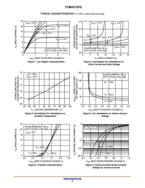
● Max RDS(on) = 30 mW at VGS = −4.5 V, ID = −7.8 A● Max RDS(on) = 37 mW at VGS = −2.5 V, ID = −6.6 A
● Max RDS(on) = 50 mW at VGS = −1.8 V, ID = −5.5 A
● Max RDS(on) = 90 mW at VGS = −1.5 V, ID = −2.0 A
● Low Profile − 0.8 mm Maximum in the New Package MicroFET 2x2 mm
● HBM ESD Protection Level > 3 kV Typical (Note 3)
● Free from Halogenated Compounds and Antimony Oxides
● This Device is Pb−Free, Halide Free and is RoHS Compliant MOSFET
MAXIMUM RATINGS
(TA = 25°C, unless otherwise noted) Symbol Parameter Ratings Unit VDS Drain to Source Voltage VGS Gate to Source Voltage ID Drain Current − Continuous (Note 1a) − Pulsed −20 V ±8 V A −7.8 −24 PD Power Dissipation Power Dissipation (Note 1a) (Note 1b) 2.4 W 0.9 TJ, TSTG Operating and Storage Junction Temperature Range −55 to +150 °C Stresses exceeding those listed in theMAXIMUM RATINGS
table may damage the device.