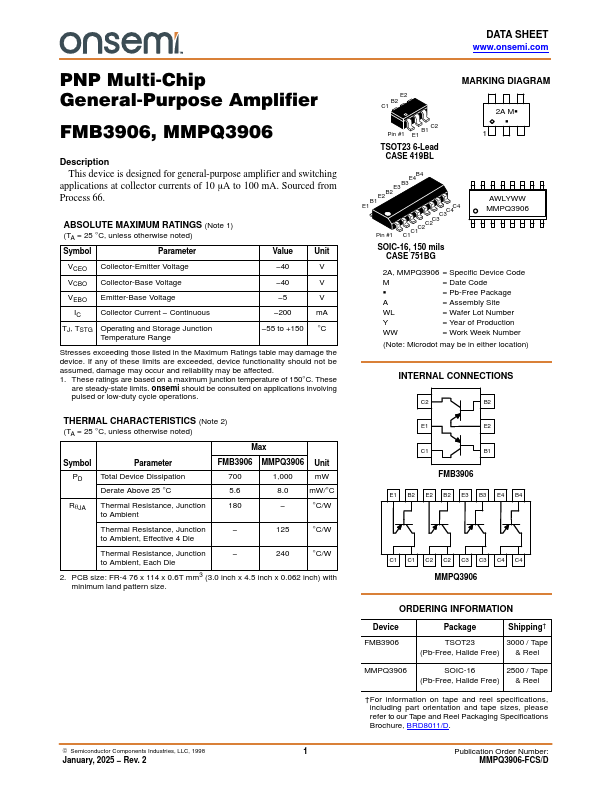
FMB3906
Description
This device is designed for general-purpose amplifier and switching applications at collector currents of 10 m A to 100 m A. Sourced from Process 66.
ABSOLUTE MAXIMUM RATINGS (Note 1) (TA = 25 °C, unless otherwise noted)
Symbol
Parameter
Value
Unit
VCEO Collector-Emitter Voltage
VCBO Collector-Base Voltage VEBO Emitter-Base Voltage
IC Collector Current
- Continuous TJ, TSTG Operating and Storage Junction
Temperature Range
- 40
- 40
- 5
- 200 m A
- 55 to +150 °C
Stresses exceeding those listed in the Maximum Ratings table may damage the device. If any of these limits are exceeded, device functionality should not be assumed, damage may occur and reliability may be affected. 1. These ratings are based on a maximum junction temperature of 150°C. These are steady-state limits. onsemi should be consulted on applications involving pulsed or low-duty cycle operations.
THERMAL CHARACTERISTICS (Note 2) (TA = 25 °C, unless otherwise noted)
Max
Symbol PD
Parameter...