onsemi HBL1009
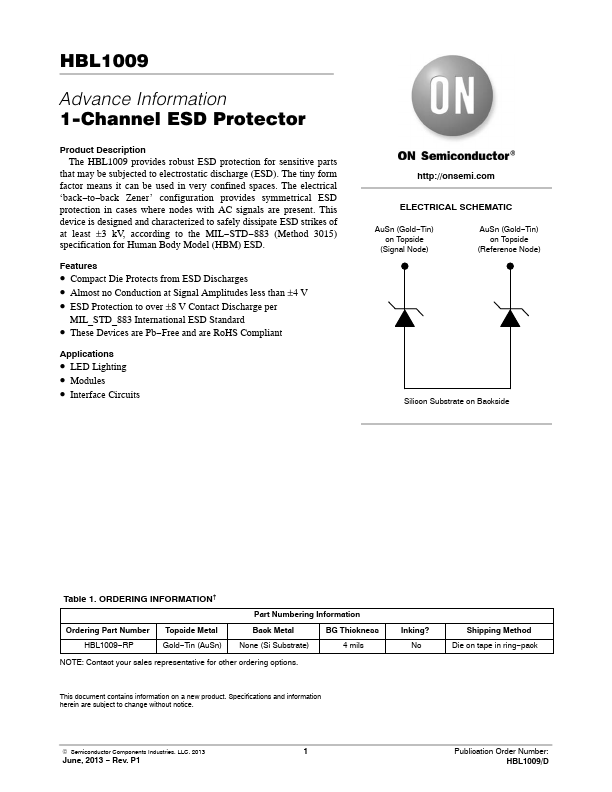
The HBL1009 provides robust ESD protection for sensitive parts that may be subjected to electrostatic discharge (ESD). The tiny form factor means it can be used in very confined spaces. The electrical ‘back−to−back Zener’ configuration provides symmetrical ESD protection in cases where nodes with AC signals are present.| Part No. | HBL1009 |
|---|---|
| Datasheet | HBL1009 Download |
| Manufacturer |  onsemi |
| Description | 1-Channel ESD Protector |
| Buy | Stock & Price |
DESCRIPTION
This device is designed and characterized to safely dissipate ESD strikes of at least ±3 kV, according to the MIL−STD−883 (Method 3015) specification for Human Body Model (HBM) ESD.FEATURES
● Compact Die Protects from ESD Discharges● Almost no Conduction at Signal Amplitudes less than ±4 V
● ESD Protection to over ±8 V Contact Discharge per MIL_STD_883 International ESD Standard
● These Devices are Pb−Free and are RoHS Compliant
APPLICATIONS
● LED Lighting● Modules
● Interface Circuits ELECTRICAL SCHEMATIC AuSn (Gold−Tin) on Topside (Signal Node) AuSn (Gold−Tin) on Topside (Reference Node) Silicon Substrate on Backside Table 1. ORDERING INFORMATION† Ordering Part Number HBL1009−RP Topside Metal Gold−Tin (AuSn) Part Numbering Information Back Metal BG Thickness None (Si Substrate) 4 mils NOTE: Contact your sales representative for other ordering options. Inking? No Shipping Method Die on tape in ring−pack This document contains information on a new product. Specifications and information herein are subject to change without notice. © Semiconductor Components Industries, LLC, 2013 June, 2013 − Rev.