DESCRIPTION
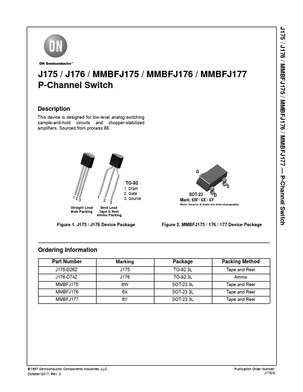
Sourced from process 88. 123 Straight Lead Bulk Packing 12 3 TO-92 1. Drain 2. Gate 3. Source Bent Lead Tape & Reel Ammo Packing Figure 1. J175 / J176 Device Package G S SOT-23 D Mark: 6W / 6X / 6Y Note: Source & drain are interchangeable. Figure 2. MMBFJ175 / 176 / 177 Device Package Ordering Information Part Number J175-D26Z J176-D74Z MMBFJ175 MMBFJ176 MMBFJ177 Marking J175 J176 6W 6X 6Y Package TO-92 3L TO-92 3L SOT-23 3L SOT-23 3L SOT-23 3L Packing Method Tape and Reel Ammo Tape and Reel Tape and Reel Tape and Reel ©1997 Semiconductor Components Industries, LLC. October-2017, Rev. 2 Publication Order Number: J175/D J175 / J176 / MMBFJ175 / MMBFJ176 / MMBFJ177 — P-Channel Switch ABSOLUTE MAXIMUM RATINGS
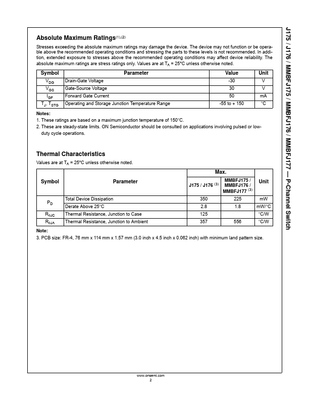
(1),(2) Stresses exceeding the absolute maximum ratings may damage the device. The device may not function or be operable above the recommended operating conditions and stressing the parts to these levels is not recommended. In addition, extended exposure to stresses above the recommended operating conditions may affect device reliability. onsemi