onsemi J309
JFET VHF/UHF Amplifiers
| Part No. | J309 |
|---|---|
| Datasheet | J309 Download |
| Manufacturer |  onsemi |
| Description | JFET VHF/UHF Amplifiers |
| Buy | Stock & Price |
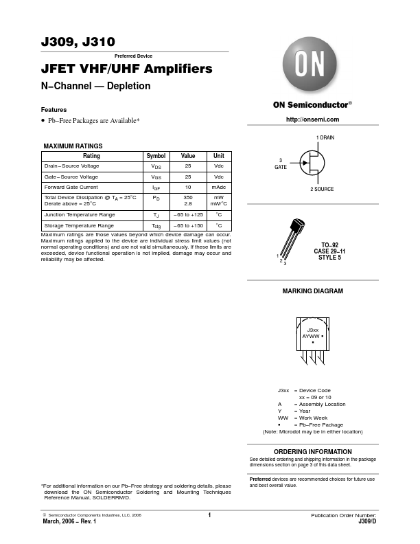
FEATURES
● Pb−Free Packages are Available*MAXIMUM RATINGS
Rating Drain −Source Voltage Gate −Source Voltage Forward Gate Current Total Device Dissipation @ TA = 25°C Derate above = 25°C Junction Temperature Range Storage Temperature Range Symbol VDS VGS IGF PD TJ Tstg Value 25 25 10 350 2.8 −65 to +125 −65 to +150 Unit Vdc Vdc mAdc mW mW/°C °C °C 1 DRAIN 3 GATE 2 SOURCE Maximum ratings are those values beyond which device damage can occur. Maximum ratings applied to the device are individual stress limit values (not normal operating conditions) and are not valid simultaneously. If these limits are exceeded, device functional operation is not implied, damage may occur and reliability may be affected. 1 2 3 TO−92 CASE 29−11 STYLE 5 MARKING DIAGRAM J3xx AYWW G G J3xx = Device Code xx = 09 or 10 A = Assembly Location Y = Year WW = Work Week G = Pb−Free Package (Note: Microdot may be in either location) ORDERING INFORMATION See detailed ordering and shipping information in the package dimensions section on page 3 of this data sheet.