onsemi LC75810E
the LC75810E and LC 75810T al so provi de on-chi p charact er di splay ROM and RAM to allo w d isplay system s to b e implemented easily. Supports accessory display segment drive (up to 80 segments) Display technique: 1/8-duty, 1/4-bias drive (5 × 7 dots, 6 × 7 dots) 1/9-duty, 1/4-bias drive (5 × 8 dots, 6 × 8 dots) 1/10-duty, 1/4-bias drive (5 × 9 dots, 6 × 9 dots) Display digits: 16 digits × 1 line (5 × 7 dots), 15 digits × 1 line (5 × 8 or 5 × 9 dots) 13 digits × 1 line (6 × 7, 6 × 8, or 6 × 9 dots) • • • • • • • • • CCB is ON Semiconductor® ’s original format.| Part No. | LC75810E |
|---|---|
| Datasheet | LC75810E Download |
| Manufacturer |  onsemi |
| Description | 1/8 to 1/10 Duty Dot Matrix LCD Display Controllers Drivers |
| Buy | Stock & Price |
FEATURES
●●
● Controls and drives a 5 × 7, 5 × 8, or 5 × 9 dot matrix LCD. All addresses are managed by ON Semiconductor® for this format.
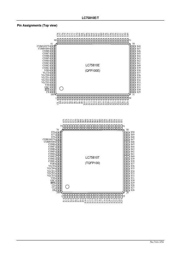
● CCB is a registered trademark of Semiconductor Components Industries, LLC. Semiconductor Components Industries, LLC, 2013 July, 2013 N2206 / 32902RM(OT)No.7141-1/54 LC75810E/T Package Dimensions unit: mm 3151A-QFP100E [LC75810E] 23.2 80 81 51 50 14.0 100 1 0.65 (0.58) 0.3 30 31 17.2 0.15 3.0max 0.1 (2.7) SANYO: QFP100E unit: mm 3274-TQFP100 [LC75810T] 0.5 16.0 14.0 75 76 51 50 100 1 (1.0) (1.0) 26 0.5 0.2 25 0.125 1.2max 0.1 14.0 16.0 SANYO: TQFP100 0.8 20.0 No.7141-2/54 LC75810E/T Pin Assignments (Top view) S78 S77 S76 S75 S74 S73 S72 S71 S70 S69 S68 S67 S66 S65 S64 S63 S62 S61 S60 S59 S58 S57 S56 S55 S54 S53 S52 S51 S50 S49 80 81 COM10/S79 COM9/S80 COM8 COM7 COM6 COM5 COM4 COM3 COM2 COM1 VDD VLCD VLCD0 VLCD1 VLCD2 VLCD3 VSS OSC RES CE 100 1 30 CL DI S1 S2 S3 S4 S5 S6 S7 S8 S9 S10 S11 S12 S13 S14 S15 S16 S17 S18 S19 S20 S21 S22 S23 S24 S25 S26 S...