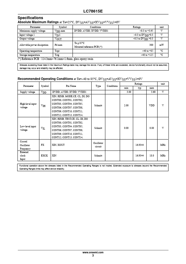
ABSOLUTE MAXIMUM RATINGS
at Ta=25°C, DVSS=AVSS=XVSS=VVSS1=0V Parameter Symbol Conditions Maximum supply voltage Input voltage 1 Output voltage VDD max VIN1 VOUT DVDD, AVDD, XVDD, VVDD1 Allowable power dissipation Pd max Ta ≤ 85°C Mounted reference PCB (*) Operating temperature Topr Storage temperature Tstg (*) Reference PCB : 114.3mm×76.1mm×1.6mm, glass epoxy resin Ratings 0.3 to +3.95 0.3 to DVDD+0.3 0.3 to DVDD +0.3 300 40 to +85 40 to +125 unit V V V mW °C °C Stresses exceeding those listed in the MAXIMUM RATINGS
table may damage the device. If any of these limits are exceeded, device functionality should not be assumed, damage may occur and reliability may be affected. Recommended Operating Conditions at Ta=40 to 85°C, DVSS=AVSS=XVSS=VVSS1=0V Parameter Symbol Pin Name Ratings Type Conditions min t onsemi