onsemi LC87F1HC4B
The LC87F1HC4B is an 8-bit microcomputer that, centered around a CPU running at a minimum bus cycle time of 83.3ns, integrates on a single chip a number of hardware features such as 128K-byte flash ROM (onboard programmable), 12288-byte RAM, an on-chip debugger, a sophisticated 16-bit timer/counter (may be divided into 8-bit timers), a 16-bit timer (may be divided into 8-bit timers or PWMs), four 8-bit timers with a prescaler, a base timer serving as a time-of-day clock, 3 channels of synchronous SIO interface with automatic data transfer capabilities, an asynchronous/synchronous SIO...| Part No. | LC87F1HC4B |
|---|---|
| Datasheet | LC87F1HC4B Download |
| Manufacturer |  onsemi |
| Description | 8-bit Microcontroller |
| Buy | Stock & Price |
FEATURES
●Flash ROM●131072 8 bits
●Capable of on-board programming with a wide range of supply voltages : 3.0 to 5.5V
●Block-erasable in 128 byte units
●Writes data in 2-byte units
●RAM
●12288 9 bits
●Package Form
● SQFP48 : Pb-Free type
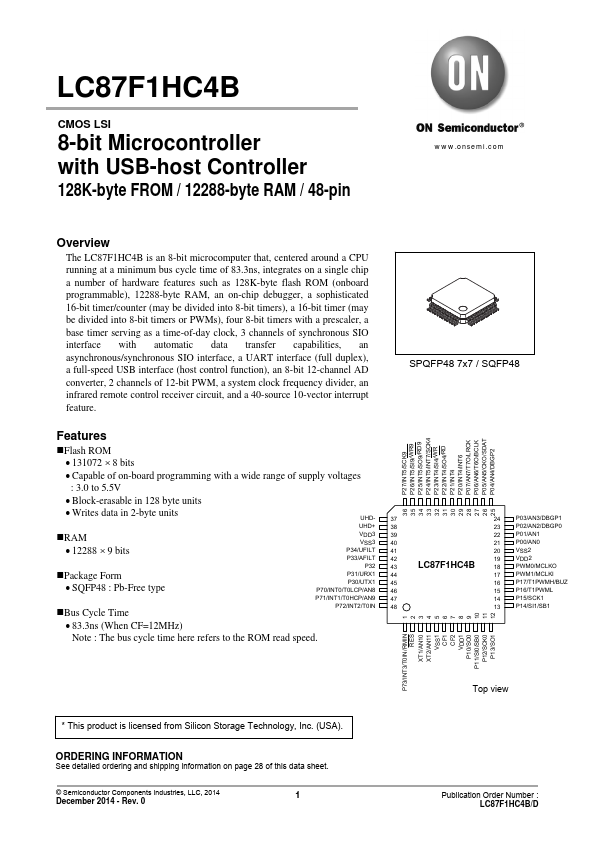
●Bus Cycle Time UHDUHD+ VDD3 VSS3 P34/UFILT P33/AFILT P32 P31/URX1 P30/UTX1 P70/INT0/T0LCP/AN8 P71/INT1/T0HCP/AN9 P72/INT2/T0IN
●83.3ns (When CF=12MHz) Note : The bus cycle time here refers to the ROM read speed. 37 38 39 40 41 42 43 44 45 46 47 48 36 35 34 33 32 31 30 29 28 27 26 25 P27/INT5/SCK9 P26/INT5/SI9/WR9 P25/INT5/SO9/RD9 P24/INT5/INT7/SCK4 P23/INT4/SI4/WR P22/INT4/SO4/RD P21/INT4 P20/INT4/INT6 P07/AN7/T7O/LRCK P06/AN6/T6O/BCLK P05/AN5/CKO/SDAT P04/AN4/DBGP2 LC87F1HC4B 24 P03/AN3/DBGP1 23 P02/AN2/DBGP0 22 P01/AN1 21 P00/AN0 20 VSS2 19 VDD2 18 PWM0/MCLKO 17 PWM1/MCLKI 16 P17/T1PWMH/BUZ 15 P16/T1PWML 14 P15/SCK1 13 P14/SI1/SB1 P73/INT3/T0IN/RMIN 1 RES 2 XT1/AN10 3 XT2/AN11 4 VSS1 5 CF1 6 CF2 7 VDD1 8 P10/SO0 9 P11/SI0/SB0 10 P12/SCK0 11 P13/SO1 12 * This product is licensed from Silicon Storage Technology, Inc. (USA).