onsemi LC87F2932A
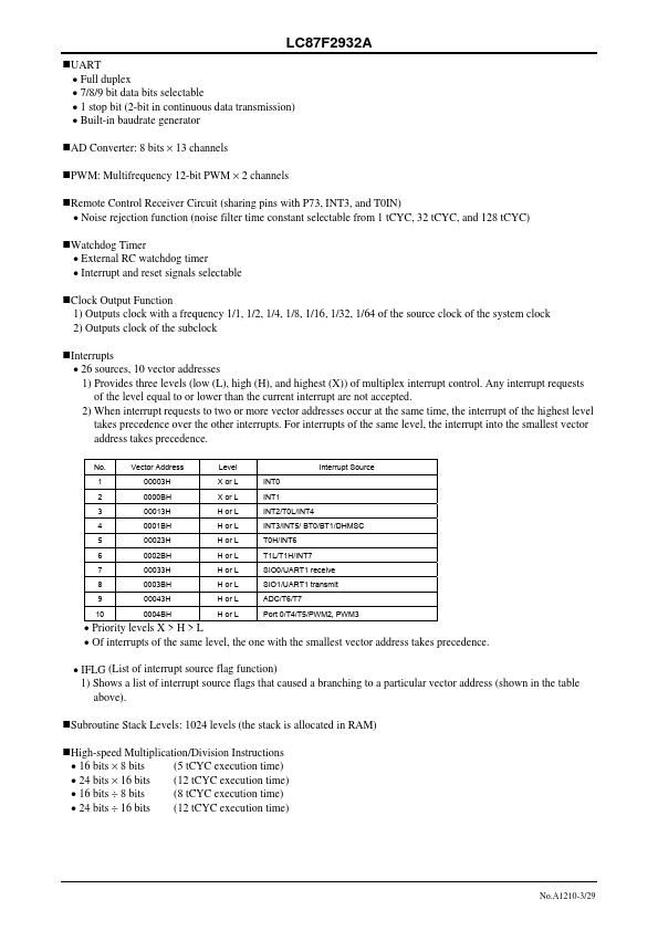
The LC87F2932A is an 8-bit microcomputer that, centered around a CPU running at a minimum bus cycle time of 83.3ns, integrates on a single chip a number of hardware features such as 32K-byte flash ROM (onboard programmable), 2048-byte RAM, an on-chip debugger, sophisticated 16-bit timers/counters (may be divided into 8bit timers), a 16-bit timer/counter (may be divided into 8-bit timers/counters or 8-bit PWMs), four 8-bit timers with a prescaler, a base timer serving as a time-of-day clock, day and time counter, a high-speed clock counter, a synchronous SIO interface (with automatic block...| Part No. | LC87F2932A |
|---|---|
| Datasheet | LC87F2932A Download |
| Manufacturer |  onsemi |
| Description | 8-bit 1-chip Microcontroller |
| Buy | Stock & Price |
FEATURES
●Flash ROM● Capable of on-board-programming with wide range, 3.0 to 5.5V, of voltage source.
● Block-erasable in 128-byte units
● Writable in 2-byte units
● 32768 × 8 bits
●RAM
● 2048 × 9 bits
●Minimum Bus Cycle
● 83.3ns (12MHz) VDD=3.0 to 5.5V
● 125ns (8MHz) VDD=2.5 to 5.5V
● 250ns (4MHz) VDD=2.2 to 5.5V Note: The bus cycle time here refers to the ROM read speed. * This product is licensed from Silicon Storage Technology, Inc. (USA). Semiconductor Components Industries, LLC, 2013 May, 2013 Ver.1.02a 91708HKIM 20080804-S00001 No.A1210-1/29
●Minimum Instruction Cycle Time
● 250ns (12MHz)
● 375ns (8MHz)
● 750ns (4MHz) VDD=3.0 to 5.5V VDD=2.5 to 5.5V VDD=2.2 to 5.5V LC87F2932A
●Ports
● Normal withstand voltage I/O ports Ports whose I/O direction can be designated in 1-bit units 59 (P0n, P1n, P2n, P30 to P33, P70 to P73, P80 to P86, PBn, PCn, PWM2, PWM3, CF2, XT2) (Ports P30 to P33 are available in FLGA68K(6.0×6.0) package only.)
● Normal withstand voltage input port 2 (CF1, XT1)
● Reset pins 1 (RES)
● Power pins 6 (VSS1 to 3, VDD1 to 3)
●Timers
● Timer 0: 16-bit timer/counter with two capture registers.