onsemi LC88F5LA4ACS
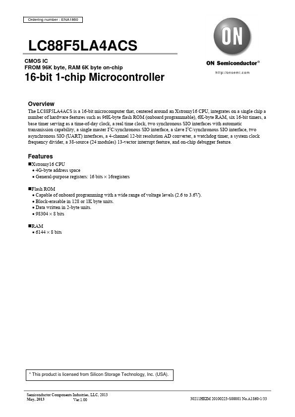
The LC88F5LA4ACS is a 16-bit microcomputer that, centered around an Xstromy16 CPU, integrates on a single chip a number of hardware features such as 96K-byte flash ROM (onboard programmable), 6K-byte RAM, six 16-bit timers, a base timer serving as a time-of-day clock, a real time clock, two synchronous SIO interfaces with automatic transmission capability, a single master I2C/synchronous SIO interface, a slave I2C/synchronous SIO interface, two asynchronous SIO (UART) interfaces, a 4-channel 12-bit resolution AD converter, a watchdog timer, a system clock frequency divider, a 38-source (24...| Part No. | LC88F5LA4ACS |
|---|---|
| Datasheet | LC88F5LA4ACS Download |
| Manufacturer |  onsemi |
| Description | 16-bit 1-chip Microcontroller |
| Buy | Stock & Price |
FEATURES
●Xstromy16 CPU● 4G-byte address space
● General-purpose registers: 16 bits × 16registers
●Flash ROM
● Capable of onboard programming with a wide range of voltage levels (2.6 to 3.6V).
● Block-erasable in 128 or 1K byte units.
● Data written in 2-byte units.
● 98304 × 8 bits
●RAM
● 6144 × 8 bits * This product is licensed from Silicon Storage Technology, Inc. (USA). Semiconductor Components Industries, LLC, 2013 May, 2013 Ver.1.00 30211HKIM 20100223-S00001 No.A1860-1/33 LC88F5LA4ACS
●Minimum instruction cycle time (tCYC)
● 100ns (10MHz) VDD = 2.6 to 3.6V
● 250ns (4MHz) VDD = 2.2 to 3.6V
●Ports
● Normal withstand voltage I/O ports Ports whose I/O direction can be designated in 1 bit units : 33 (P0n P1n, P20 to P25, P3n, P60 to P62)
● Oscillation/normal withstand voltage I/O ports : 2 (PC0, PC1)
● Oscillation pins : 2 (CF1, CF2)
● Reset pins : 1 (RESB)
● TEST pins : 1 (TEST)
● Power pins : 7 (VSS1 to 2, VSSA, VDD1 to 3, VDDA)
●Timers
● Timer 0: 16-bit timer that supports PWM/tog...