onsemi LM301A
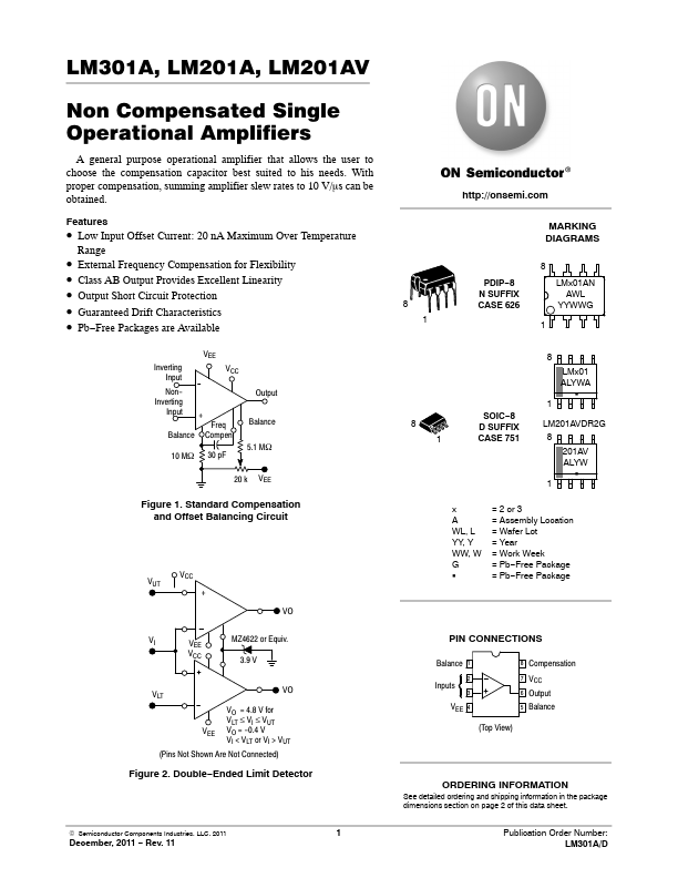
Non Compensated Single Operational Amplifiers
| Part No. | LM301A |
|---|---|
| Datasheet | LM301A Download |
| Manufacturer |  onsemi |
| Description | Non Compensated Single Operational Amplifiers |
| Buy | Stock & Price |
FEATURES
● Low Input Offset Current: 20 nA Maximum Over Temperature Range● External Frequency Compensation for Flexibility
● Class AB Output Provides Excellent Linearity
● Output Short Circuit Protection
● Guaranteed Drift Characteristics
● Pb−Free Packages are Available Inverting Input VEE VCC NonInverting Input + Freq Balance Compen 10 MW 30 pF Output Balance 5.1 MW 20 k VEE Figure 1. Standard Compensation and Offset Balancing Circuit VUT VCC + VI VEE VCC VO MZ4622 or Equiv. 3.9 V VLT VO VO = 4.8 V for VLT ≤ VI ≤ VUT VEE VO = -0.4 V VI < VLT or VI > VUT (Pins Not Shown Are Not Connected) Figure 2. Double−Ended Limit Detector © Semiconductor Components Industries, LLC, 2011 Decemb