onsemi LM311
Single Comparators
| Part No. | LM311 |
|---|---|
| Datasheet | LM311 Download |
| Manufacturer |  onsemi |
| Description | Single Comparators |
| Buy | Stock & Price |
FEATURES
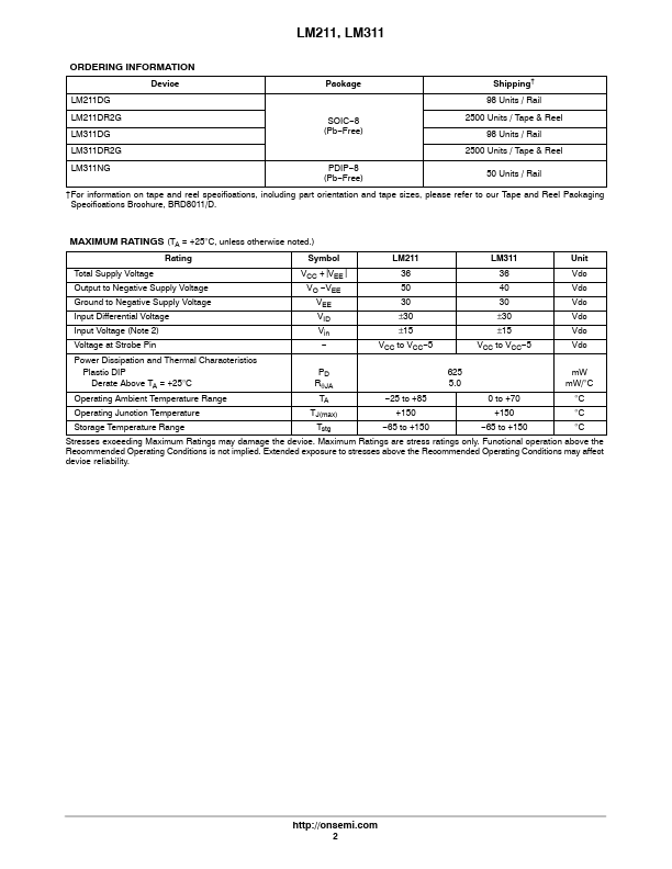
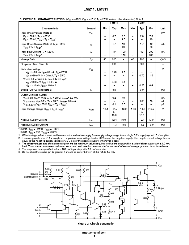
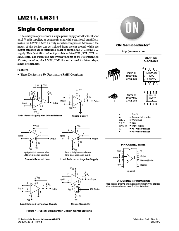
● These Devices are Pb−Free and are RoHS Compliant 3.0 k VCC 5.0 k 5 2 + 6 87 Inputs 3 − 1 RL Inputs Output 4 VEE Split Power Supply with Offset Balance VCC 2 8 + 7 3 - 1 VEE 4 RL Output Single Supply 2 Inputs 3 VCC +8 7 −1 4 RL Output VEE Input polarity is reversed when GND pin is used as an output. Ground−Referred Load VCC Inputs 2 + 8 7 3− 1 4 RL Output VEE Input polarity is reversed when GND pin is used as an output. Load Referred to Negative Supply VCC Inputs 2 + 3− 4 VEE VCC 8 7 1 2+ 8 7 Inputs 3 − 1 RL 6 4 Output VEE RL Output TTL Strobe 1.0 k Load Referred to Positive Supply Strobe Capability Figure 1. Typical Comparator Design Configurations 8 1 8 1 MARKING DIAGRAMS PDIP−8 N SUFFIX CASE 626 8 LM311AN AWL YYWWG 1 SOIC−8 D SUFFIX CASE 751 8 LMx11 ALYW G 1 x A WL, L YY, Y WW, W G G = 2 or 3 = Assembly Location = Wafer Lot = Year = Work Week = Pb−Free Package = Pb−Free Package PIN CONNECTIONS GND 1 2 Inputs + 3− VEE 4 8 VCC 7 Output 6 Balance/Strobe 5 Balance (Top View) O...