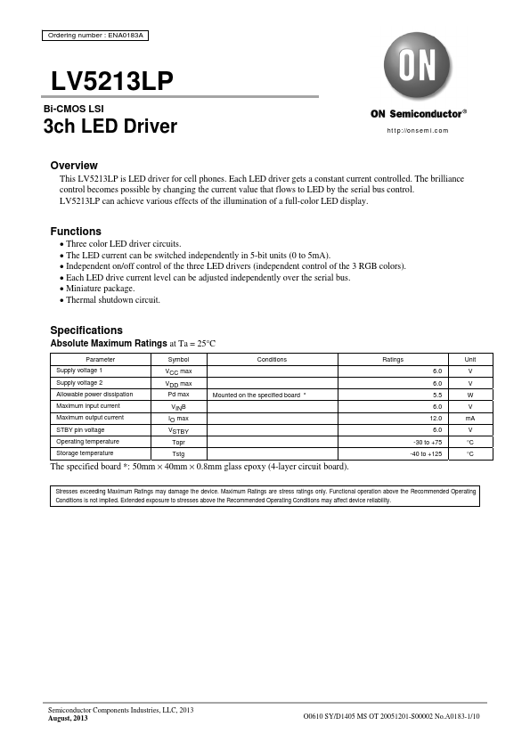
ABSOLUTE MAXIMUM RATINGS
at Ta = 25°C Parameter Symbol Conditions Supply voltage 1 Supply voltage 2 Allowable power dissipation VCC max VDD max Pd max Mounted on the specified board * Maximum input current Maximum output current STBY pin voltage Operating temperature VINB IO max VSTBY Topr Storage temperature Tstg The specified board *: 50mm × 40mm × 0.8mm glass epoxy (4-layer circuit board). Ratings 6.0 6.0 5.5 6.0 12.0 6.0 -30 to +75 -40 to +125 Unit V V W V mA V °C °C Stresses exceeding MAXIMUM RATINGS
may damage the device. MAXIMUM RATINGS
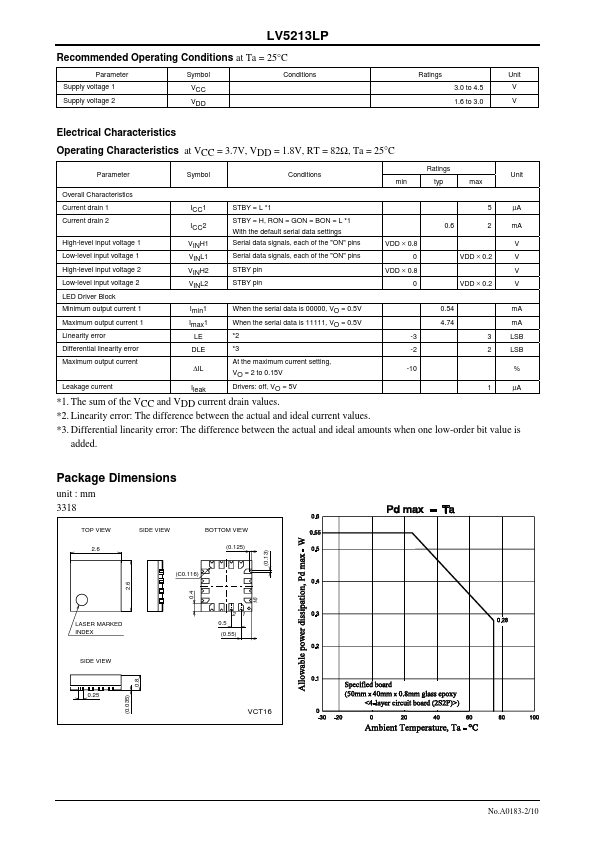
are stress ratings only. Functional operation above the Recommended Operating Conditions is not implied. Extended exposure to stresses above the Recommended Operating Conditions may affect device reliability. Semiconductor Components Industries, LLC, 2013 August, 2013 O0610 SY/D1405 MS OT 20051201-S00002 No.A0183-1/10 LV5213LP Recommended Operating Conditions at Ta = 25°C Parameter Supply voltage 1 Supply voltage 2 Symbol VCC VDD Conditions Ratin... onsemi