ABSOLUTE MAXIMUM RATINGS
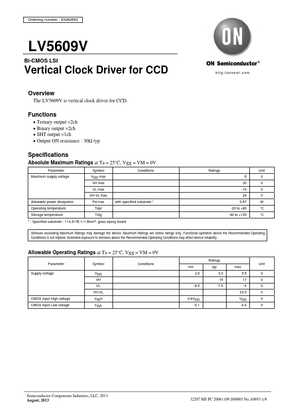
at Ta = 25°C, VSS = VM = 0V Parameter Symbol Conditions Maximum supply voltage VDD max VH max VL max VH-VL max Allowable power dissipation Pd max with specified substrate * Operating temperature Topr Storage temperature Tstg * : Specified substrate : 114.3×76.1×1.6mm3, glass epoxy board Ratings 6 20 -10 24 0.67 -20 to +80 -40 to +125 Unit V V V V W °C °C Stresses exceeding MAXIMUM RATINGS
may damage the device. MAXIMUM RATINGS
are stress ratings only. Functional operation above the Recommended Operating Conditions is not implied. Extended exposure to stresses above the Recommended Operating Conditions may affect device reliability. Allowable Operating Ratings at Ta = 25°C, VSS = VM = 0V Parameter Symbol Conditions Supply voltage CMOS input High voltage CMOS input Low voltage VDD VH VL VH-VL VINH VINL min 2.0 -8.5 Ratings typ 3.3 15 -7.5 0.8VDD -0.1 max 5.5 17 -4 23.5 VDD 0.4 Unit V V V V V V Semiconductor Components Industries, LLC, 2013 August, 2013 32207 MS P... onsemi