onsemi M75N06HD
Power MOSFET
| Part No. | M75N06HD |
|---|---|
| Datasheet | M75N06HD Download |
| Manufacturer |  onsemi |
| Description | Power MOSFET |
| Buy | Stock & Price |
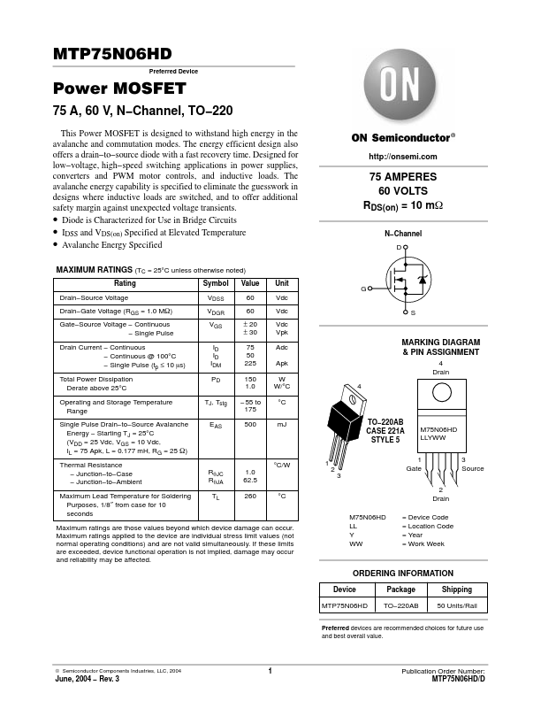
MAXIMUM RATINGS
(TC = 25°C unless otherwise noted) Rating Symbol Value Unit Drain−Source Voltage Drain−Gate Voltage (RGS = 1.0 MW) Gate−Source Voltage − Continuous Gate−Source Voltage − Single Pulse VDSS VDGR VGS 60 60 ± 20 ± 30 Vdc Vdc Vdc Vpk Drain Current − Continuous Drain Current − Continuous @ 100°C Drain Current − Single Pulse (tp ≤ 10 ms) Total Power Dissipation Derate above 25°C ID 75 Adc ID 50 IDM 225 Apk PD 150 W 1.0 W/°C Operating and Storage Temperature Range TJ, Tstg −55 to 175 °C Single Pulse Drain−to−Source Avalanche Energy − Starting TJ = 25°C (VDD = 25 Vdc, VGS = 10 Vdc, IL = 75 Apk, L = 0.177 mH, RG = 25 W) Thermal Resistance − Junction−to−Case − Junction−to−Ambient EAS RqJC RqJA 500 mJ °C/W 1.0 62.5 Maximum Lead Temperature for Soldering Purposes, 1/8″ from case for 10 seconds TL 260 °C Maximum ratings are those values beyond which device damage can occur. Maximum ratings applied to the device are individual stress limit values (not normal operating conditions) and are not valid simultaneously.