onsemi MC100LVEL40
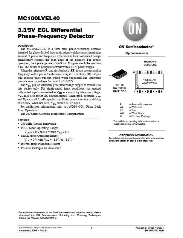
The MC100LVEL40 is a three state phase frequency−detector intended for phase−locked loop applications which require a minimum amount of phase and frequency difference at lock. For proper operation, the input edge rate of the R and V inputs should be less than 5 ns. The device is designed to work with a 3.3 V power supply.| Part No. | MC100LVEL40 |
|---|---|
| Datasheet | MC100LVEL40 Download |
| Manufacturer |  onsemi |
| Description | Phase-Frequency Detector |
| Buy | Stock & Price |
DESCRIPTION
Advanced design significantly reduces the dead zone of the detector. When the reference (R) and the feedback (FB) inputs are unequal in frequency and/or phase the differential up (U) and down (D) outputs will provide pulse streams which when subtracted and integrated provide an error voltage for control of a VCO. The VBB pin, an internally generated voltage supply, is available to this device only. For single-ended input conditions, the unused differential input is connected to VBB as a switching reference voltage. VBB may also rebias AC coupled inputs. When used, decouple VBB and VCC via a 0.01 mF capacitor and limit current sourcing or sinking to 0.5 mA. When not used, VBB should be left open. For application information, refer to AND8040/D, “Phase Lock Loop Operation.” The 100 Series Contains Temperature CompensationFEATURES
MARKING DIAGRAM 20 20 1 SO−20 DW SUFFIX CASE 751D 100LVEL40 AWLYYWWG 1 A WL YY WW G = Assembly Location = Wafer Lot = Year = Work Week = Pb−Free Package● 250 MHz Typical Bandwidth
● PECL Mode Operating Range: *For additional marking information, refer to Application Note AND8002/D.