onsemi MC14012B
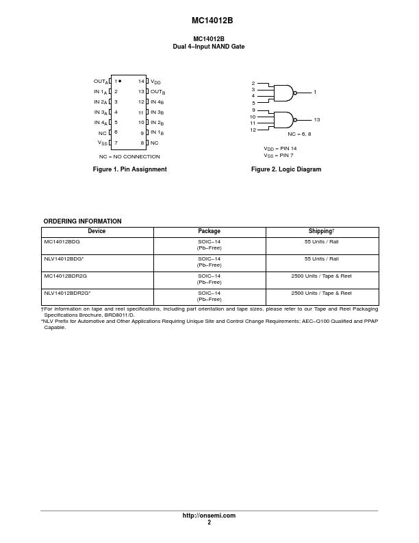
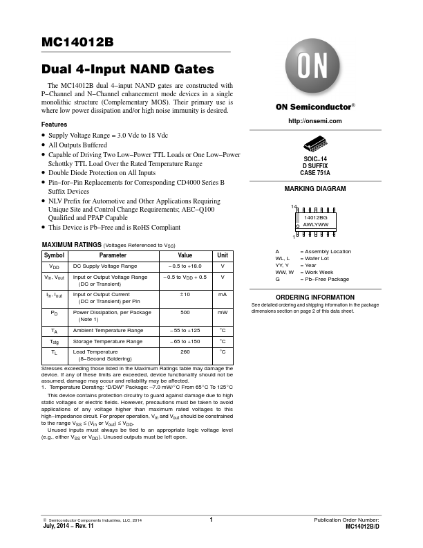
The MC14012B dual 4−input NAND gates are constructed with P−Channel and N−Channel enhancement mode devices in a single monolithic structure (Complementary MOS).| Part No. | MC14012B |
|---|---|
| Datasheet | MC14012B Download |
| Manufacturer |  onsemi |
| Description | Dual 4-Input NAND Gates |
| Buy | Stock & Price |
FEATURES
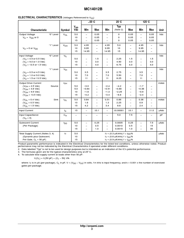
● Supply Voltage Range = 3.0 Vdc to 18 Vdc● All Outputs Buffered
● Capable of Driving Two Low−Power TTL Loads or One Low−Power Schottky TTL Load Over the Rated Temperature Range
● Double Diode Protection on All Inputs
● Pin−for−Pin Replacements for Corresponding CD4000 Series B Suffix Devices
● NLV Prefix for Automotive and Other
APPLICATIONS
Requiring Unique Site and Control Change Requirements; AEC−Q100 Qualified and PPAP Capable● This Device is Pb−Free and is RoHS Compliant
MAXIMUM RATINGS
(Voltages Referenced to VSS) Symbol Parameter Value Unit VDD Vin, Vout DC Supply Voltage Range Input or Output Voltage Range (DC or Transient) −0.5 to +18.0 −0.5 to VDD + 0.5 V V Iin, Iout Input or Output Current (DC or Transient) per Pin ± 10 mA PD Power Dissipation, per Package (Note 1) 500 mW TA Ambient Temperature Range −55 to +125 °C Tstg Storage Temperature Range −65 to +150 °C TL Lead Temperature (8−Second Soldering) 260 °C Stresses exceeding those listed in theMAXIMUM RATINGS
table may damage the device.