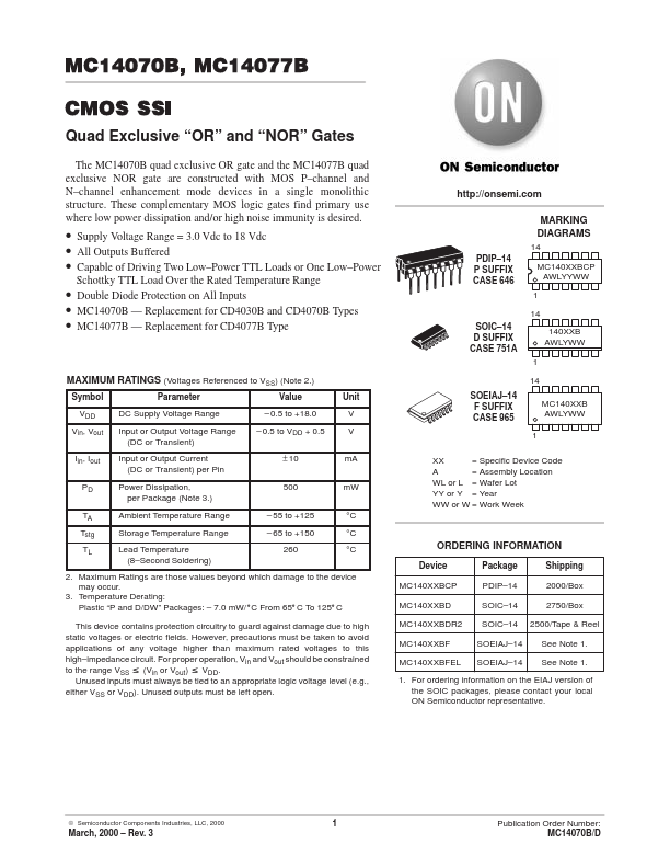
MAXIMUM RATINGS
(Voltages Referenced to VSS) (Note 2.) Symbol VDD Vin, Vout Iin, Iout PD TA Tstg TL Parameter DC Supply Voltage Range Input or Output Voltage Range (DC or Transient) Input or Output Current (DC or Transient) per Pin Power Dissipation, per Package (Note 3.) Ambient Temperature Range Storage Temperature Range Lead Temperature (8–Second Soldering) Value – 0.5 to +18.0 – 0.5 to VDD + 0.5 ± 10 500 – 55 to +125 – 65 to +150 260 Unit V V mA mW °C °C °C SOEIAJ–14 F SUFFIX CASE 965 14 MC140XXB AWLYWW 1 XX = Specific Device Code A = Assembly Location WL or L = Wafer Lot YY or Y = Year WW or W = Work Week ORDERING INFORMATION Device MC140XXBCP MC140XXBD MC140XXBDR2 MC140XXBF MC140XXBFEL Package PDIP–14 SOIC–14 SOIC–14 SOEIAJ–14 SOEIAJ–14 Shipping 2000/Box 2750/Box 2500/Tape & Reel See Note 1. See Note 1. 2. MAXIMUM RATINGS
are those values beyond which damage to the device may occur. 3. Temperature Derating: Plastic “P and D/DW” Packages: – 7.0 mW/_C From 65_C To 125_C This device contains protection circuitry to guard against damage due to high static voltages or electric fields. onsemi