onsemi MC14081B
CMOS Gates
| Part No. | MC14081B |
|---|---|
| Datasheet | MC14081B Download |
| Manufacturer |  onsemi |
| Description | CMOS Gates |
| Buy | Stock & Price |
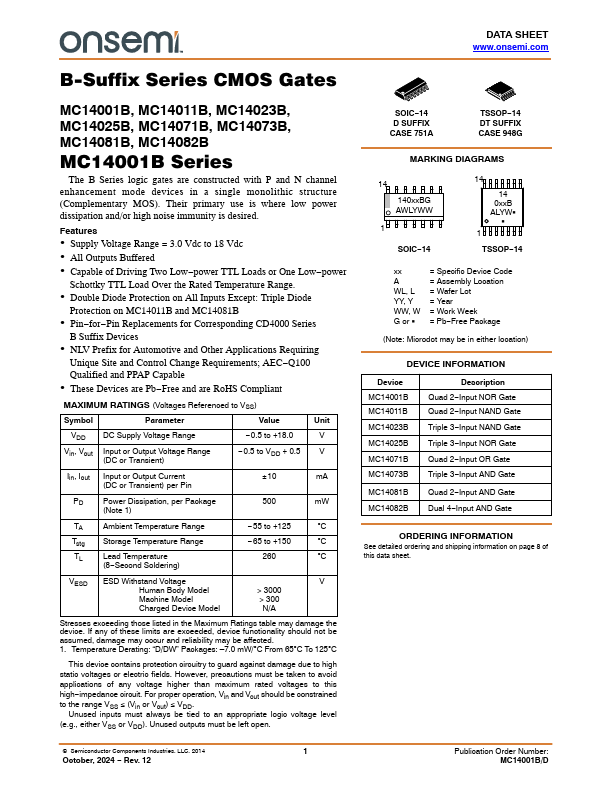
FEATURES
● Supply Voltage Range = 3.0 Vdc to 18 Vdc● All Outputs Buffered
● Capable of Driving Two Low−power TTL Loads or One Low−power Schottky TTL Load Over the Rated Temperature Range.
● Double Diode Protection on All Inputs Except: Triple Diode Protection on MC14011B and MC14081B
● Pin−for−Pin Replacements for Corresponding CD4000 Series B Suffix Devices
● NLV Prefix for Automotive and Other
APPLICATIONS
Requiring Unique Site and Control Change Requirements; AEC−Q100 Qualified and PPAP Capable● These Devices are Pb−Free and are RoHS Compliant
MAXIMUM RATINGS
(Voltages Referenced to VSS) Symbol Parameter Value Unit VDD Vin, Vout DC Supply Voltage Range Input or Output Voltage Range (DC or Transient) −0.5 to +18.0 V −0.5 to VDD + 0.5 V Iin, Iout Input or Output Current (DC or Transient) per Pin 10 mA PD Power Dissipation, per Package (Note 1) 500 mW TA Ambient Temperature Range Tstg Storage Temperature Range TL Lead Temperature (8−Second Soldering) −55 to +125 C −65 to +150 C 2...
