onsemi MC14094B
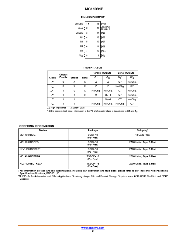
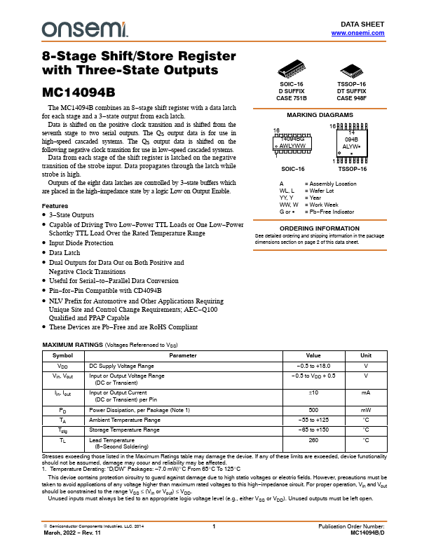
The MC14094B combines an 8−stage shift register with a data latch for each stage and a 3−state output from each latch. The QS output data is for use in high−speed cascaded systems. The QS output data is shifted on the following negative clock transition for use in low−speed cascaded systems.| Part No. | MC14094B |
|---|---|
| Datasheet | MC14094B Download |
| Manufacturer |  onsemi |
| Description | 8-Stage Shift/Store Register |
| Buy | Stock & Price |
FEATURES
● 3−State Outputs● Capable of Driving Two Low−Power TTL Loads or One Low−Power Schottky TTL Load Over the Rated Temperature Range
● Input Diode Protection
● Data Latch
● Dual Outputs for Data Out on Both Positive and Negative Clock Transitions
● Useful for Serial−to−Parallel Data Conversion
● Pin−for−Pin Compatible with CD4094B
● NLV Prefix for Automotive and Other
APPLICATIONS
Requiring Unique Site and Control Change Requirements; AEC−Q100 Qualified and PPAP Capable● These Devices are Pb−Free and are RoHS Compliant SOIC−16 D SUFFIX CASE 751B TSSOP−16 DT SUFFIX CASE 948F MARKING DIAGRAMS 16 14094BG AWLYWW 1 SOIC−16 16 14 094B ALYWG G 1 TSSOP−16 A WL, L YY, Y WW, W G or G = Assembly Location = Wafer Lot = Year = Work Week = Pb−Free Indicator ORDERING INFORMATION See detailed ordering and shipping information in the package dimensions section on page 2 of this data sheet.
MAXIMUM RATINGS
(Voltages Referenced to VSS) Symbol Parameter Value Unit VDD Vin, Vout DC Supply Voltage R...