onsemi MC3488A
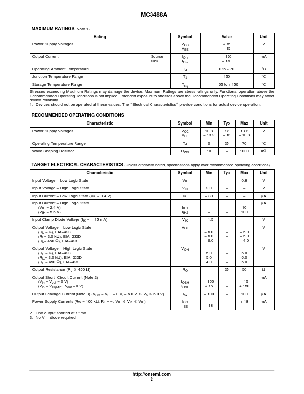
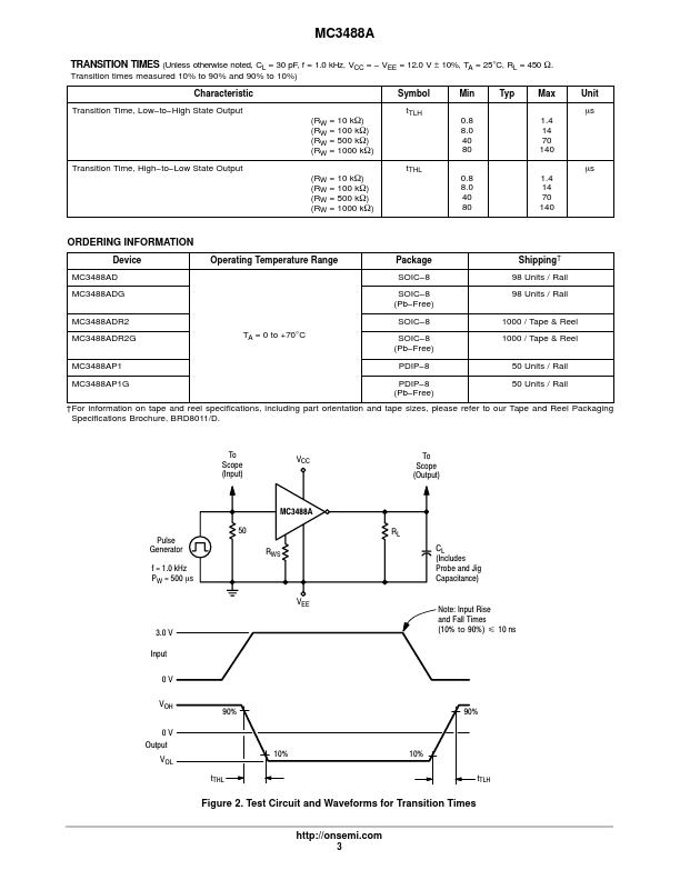
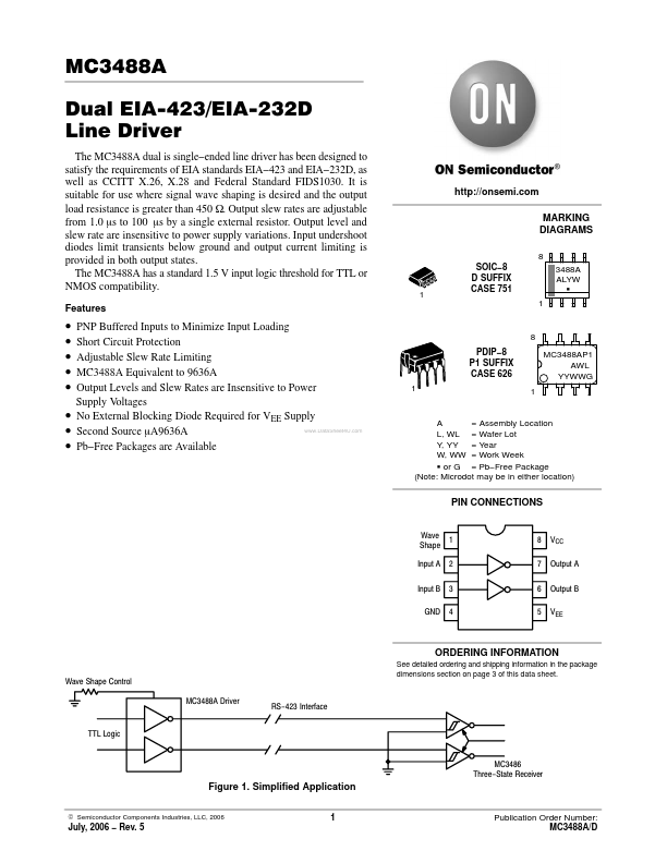
The MC3488A dual is single−ended line driver has been designed to satisfy the requirements of EIA standards EIA−423 and EIA−232D, as well as CCITT X.26, X.28 and Federal Standard FIDS1030. It is suitable for use where signal wave shaping is desired and the output load resistance is greater than 450 W. The MC3488A has a standard 1.5 V input logic threshold for TTL or NMOS compatibility.| Part No. | MC3488A |
|---|---|
| Datasheet | MC3488A Download |
| Manufacturer |  onsemi |
| Description | Dual EIA-423/EIA-232D Line Driver |
| Buy | Stock & Price |
FEATURES
MARKING DIAGRAMS 8 SOIC−8 D SUFFIX CASE 751 1 3488A ALYW G 1●
●
●
●
●
●
●
● PNP Buffered Inputs to Minimize Input Loading Short Circuit Protection Adjustable Slew Rate Limiting MC3488A Equivalent to 9636A Output Levels and Slew Rates are Insensitive to Power Supply Voltages No External Blocking Diode Required for VEE Supply Second Source mA9636A Pb−Free Packages are Available 8 PDIP−8 P1 SUFFIX CASE 626 1 1 MC3488AP1 AWL YYWWG A = Assembly Location L, WL = Wafer Lot Y, YY = Year W, WW = Work Week G or G = Pb−Free Package (Note: Microdot may be in either location) PIN CONNECTIONS Wave 1 Shape Input A 2 Input B 3 GND 4 8 7 6 5 VCC Output A Output B VEE ORDERING INFORMATION Wave Shape Control MC3488A Driver RS−423 Interface See detailed ordering and shipping information in the package dimensions section on page 3 of this data sheet. TTL Logic MC3486 Three−State Receiver Figure 1. Simplified Application © Semiconductor Components Industries, LLC, 2006 1 July, 2006 − Rev. 5 Public...